

| Distributor | Stock | Pricing | MOQ | PKG | Lead Time | Date Code | On Order Quantity | On Order Delivery | |
|---|---|---|---|---|---|---|---|---|---|
|
2,500 pcs
|
2500 pcs | On Request | 1 | On Request | On Request | On Request | On Request | On Request |
| Category | |
| Manufacturer Name | |
| Architecture | |
| Data Interface | |
| Differential Output | |
| INL | |
| Mounting Type | |
| Number of Bits | |
| Number of D | |
| Operating Temperature | |
| Output Type | |
| Reference Type | |
| SVHC Present | |
| Settling Time | |
| Supplier Device Package | |
| Voltage |
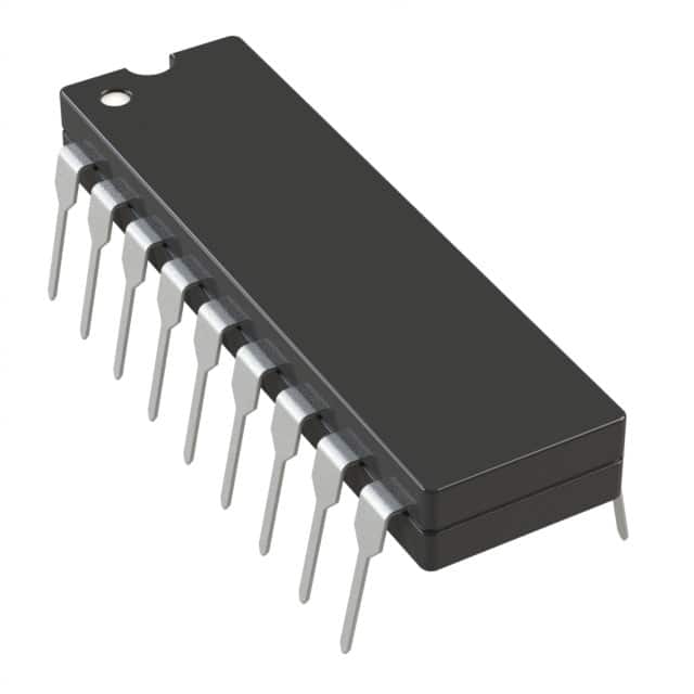
The AD7248JN is a complete 12-bit digital-to-analog converter from Analog Devices, integrating a DAC, output amplifier, and internal voltage reference on a single CMOS chip. It provides a buffered voltage output and requires no external trims for full specified performance.
Key specifications include 12-bit resolution with ±1 LSB maximum INL/DNL, a typical settling time of 5µs, and operation from a 14.25V to 15.75V supply. The parallel data interface allows easy connection to microprocessors, and the internal reference simplifies design.
The R-2R ladder architecture ensures monotonic performance. The device supports single or dual supply operation and consumes low power (65mW typical). The buffered output can drive loads directly.
Housed in a 20-pin DIP (0.300" width) with through-hole mounting, the AD7248JN is suitable for breadboarding and prototyping. Operating temperature range is 0°C to 70°C, making it ideal for commercial applications.
14.25V to 15.75V.
20-DIP (0.300", 7.62mm).
0°C to 70°C.
RoHS3 Compliant (unverified).
12 bits.
5 µs typical.
Parallel.