

| Distributor | Stock | Pricing | MOQ | PKG | Lead Time | Date Code | On Order Quantity | On Order Delivery | |
|---|---|---|---|---|---|---|---|---|---|
|
6 pcs
|
6 pcs | On Request | 1 | On Request | On Request | 92 | On Request | On Request |
| Category | |
| Manufacturer Name | |
| Architecture | |
| Configuration | |
| Data Interface | |
| Features | |
| Input Type | |
| Lead Style | |
| Mounting Type | |
| Number of A | |
| Number of Bits | |
| Number of Inputs | |
| Operating Temperature | |
| Reference Type | |
| Supplier Device Package | |
| Voltage |
The AD670JP is a complete 8-bit signal conditioning analog-to-digital converter from Analog Devices / Maxim Integrated. It integrates an instrumentation amplifier front end, a successive approximation register (SAR) ADC, a precision voltage reference, and a three-state output buffer on a single monolithic chip. The device requires no external components or user trims for full accuracy operation.
The ADC accepts differential inputs and supports two input voltage ranges: 0 mV to 255 mV (1 mV/LSB) and 0 V to 2.55 V (10 mV/LSB). It features a typical conversion time of 10 µs and operates from a single +5 V supply. The architecture is SAR with an internal reference type.
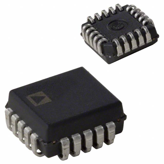
The AD670JP is housed in a 20-LCC (J-Lead) surface-mount package, specifically a 20-PLCC (9x9) supplier device package. It is designed for applications requiring high common-mode rejection and direct interface to transducers.
The AD670JP is an 8-bit analog-to-digital converter.
The typical conversion time is 10 µs.
The supply voltage is 5 V.
The AD670JP is available in a 20-LCC (J-Lead) package, specifically a 20-PLCC (9x9) surface-mount package.
The operating temperature range is 0°C to 70°C.
The AD670JP uses a successive approximation register (SAR) architecture.
Yes, the AD670JP has an internal reference type.