


| Distributor | Stock | Pricing | MOQ | PKG | Lead Time | Date Code | On Order Quantity | On Order Delivery | |
|---|---|---|---|---|---|---|---|---|---|
|
6,500 pcs
|
6500 pcs | On Request | 1 | On Request | On Request | On Request | On Request | On Request |
| Category | |
| Manufacturer Name | |
| Architecture | |
| Configuration | |
| Data Interface | |
| Input Type | |
| Mounting Type | |
| Number of A | |
| Number of Bits | |
| Number of Inputs | |
| Operating Temperature | |
| Ratio | |
| Reference Type | |
| Supplier Device Package | |
| Voltage |
Analog Devices AD573JNZ is a complete 10-bit successive approximation analog-to-digital converter (ADC) integrating a DAC, voltage reference, clock, comparator, successive approximation register (SAR), and three-state output buffers on a single chip.
The ADC accepts analog inputs of 0 V to +10 V (unipolar) or -5 V to +5 V (bipolar). It operates from a +5 V positive supply and a -12 V to -15 V negative supply. Conversion time is 20 µs typical. The data interface is parallel, with high byte/low byte output control.
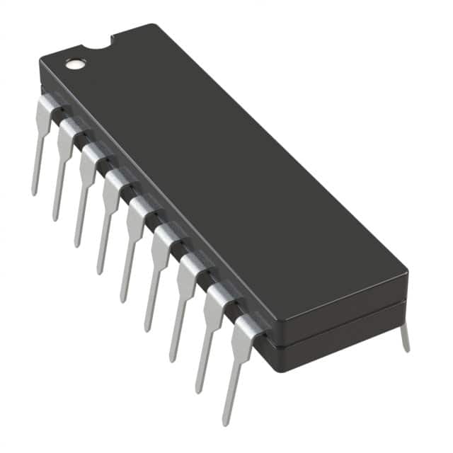
Housed in a 20-pin PDIP package with through-hole mounting, the AD573JNZ is suitable for industrial and instrumentation applications requiring moderate-speed, high-resolution analog-to-digital conversion.
The AD573JNZ requires a positive supply of +4.5V to +7V (recommended +5V) and a negative supply of -12V to -16.5V (typically -12V to -15V).
It is available in a 20-DIP (0.300", 7.62mm) package, specifically the 20-PDIP variant for through-hole mounting.
The operating temperature range is 0°C to 70°C (commercial).
The RoHS status is listed as RoHS3 Compliant, but this is unverified low-confidence data.
The AD573JNZ has a resolution of 10 bits.
It uses successive approimation (SAR) architecture.
The AD573JNZ supports two input ranges: 0V to +10V (unipolar) and -5V to +5V (bipolar).