

| Distributor | Stock | Pricing | MOQ | PKG | Lead Time | Date Code | On Order Quantity | On Order Delivery | |
|---|---|---|---|---|---|---|---|---|---|
|
3,600 pcs
|
3600 pcs | On Request | 1 | On Request | On Request | On Request | On Request | On Request |
| Category | |
| Manufacturer Name | |
| Architecture | |
| Data Interface | |
| Differential Output | |
| INL | |
| Lead Style | |
| Mounting Type | |
| Number of Bits | |
| Number of D | |
| Number of Pins | |
| Operating Temperature | |
| Output Type | |
| Power Dissipation | |
| Reference Type | |
| Settling Time | |
| Supplier Device Package | |
| Termination Style | |
| Voltage |
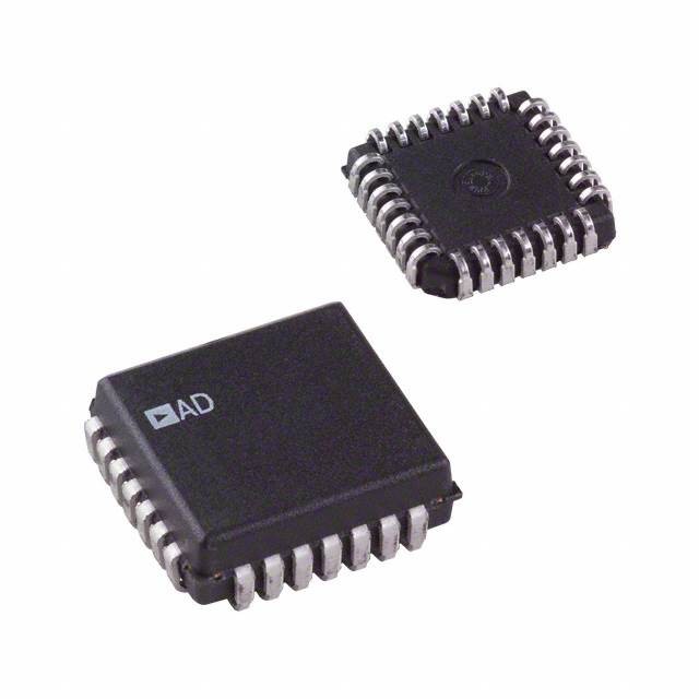
The AD569JPZ is a monolithic 16-bit digital-to-analog converter (DAC) manufactured in Analog Devices’ BiMOS II process, combining low power CMOS logic with high precision bipolar linear circuitry. The part includes two resistor strings, selector switches, decoding logic, buffer amplifiers, and double-buffered input latches. Its segmented architecture ensures 16-bit monotonicity over time and temperature.
Key electrical specifications include a typical settling time of 3 µs to within ±0.001% for a full-scale step, typical integral nonlinearity of ±0.01%, and typical differential nonlinearity of ±0.0004%. The output voltage range is ±5 V into a 1 kΩ load, and the reference input voltage range is ±5 V. The device operates from a bipolar supply of ±10.8 V to 13.2 V and consumes 800 mW typical power dissipation.
The DAC supports an external reference and is available in a 28-lead PLCC (J-Lead) surface-mount package. Operating temperature range is 0°C to 70°C. The part is suited for applications such as robotics, closed-loop positioning, and high-resolution ADC systems.
16 bits.
The supply voltage range is ±10.8V to 13.2V.
Typical settling time is 3 µs for a full-scale step, with a maximum of 6 µs.
Buffered voltage output.
The AD569JPZ is available in a 28-lead PLCC (J-Lead) surface-mount package (28-LCC).
The operating temperature range is 0°C to 70°C.
The AD569JPZ is listed as RoHS3 compliant, but this status is unverified.