

| Distributor | Stock | Pricing | MOQ | PKG | Lead Time | Date Code | On Order Quantity | On Order Delivery | |
|---|---|---|---|---|---|---|---|---|---|
|
3,600 pcs
|
3600 pcs | On Request | 1 | On Request | On Request | On Request | On Request | On Request |
| Category | |
| Manufacturer Name | |
| Architecture | |
| Data Interface | |
| Differential Output | |
| INL | |
| Lead Style | |
| Mounting Type | |
| Number of Bits | |
| Number of D | |
| Operating Temperature | |
| Output Type | |
| Reference Type | |
| SVHC Present | |
| Settling Time | |
| Supplier Device Package | |
| Voltage |
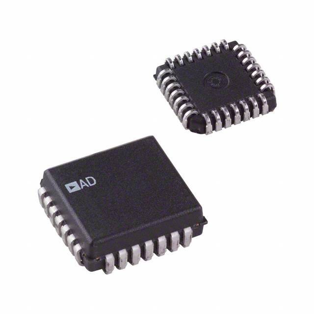
The AD569JP is a monolithic 16-bit digital-to-analog converter (DAC) manufactured in Analog Devices' BiMOS II process. It integrates two resistor strings, selector switches, decoding logic, buffer amplifiers, and double-buffered input latches on a single chip.
This DAC guarantees 16-bit monotonicity with a typical integral nonlineartiy of ±0.01% and diferential nonlineartiy of ±0.0004%. It achieves a fast settling time of 3 µs to ±0.001% for a full-scale step. The output is voltage-buffered with a range of ±5 V. The reference input is external and accepts ±5 V, allowing unipolar or bipolar operation.
Data is loaded via an 8- or 16-bit parallel interface. The double-buffered architecture simplifies bus interfacing and allows asynchronous loading of multiple DACs. The device operates from dual supplies of ±10.8 V to ±13.2 V and is specified over 0°C to 70°C.
The AD569JP is available in a 28-pin PLCC package (J-Lead) with surface mount mounting. Typical applications include robotics, closed-loop positioning, high-resolution ADC drivers, and microprocessor-based process control.
0°C to 70°C.
28-LCC (J-Lead) also known as 28-PLCC (11.51x11.51 mm).
RoHS3 compliant according to unverified data.
Dual supplies: positive 10.8V to 13.2V, negative -10.8V to -13.2V.
Parallel interface supporting 8-bit and 16-bit buses.
16 bits.
3 µs typical to ±0.001% for full-scale step.