

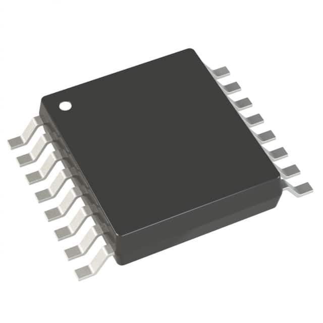
AD5317BRU The AD5317BRU is a quad 10-bit buffered voltage output DAC from Analog Devices. It features 4 channels, SPI/DSP interface, 9 µs settling time, and operates from 2.5V to 5.5V.
Mfr Part #:

AD5317BRU

Available from 1 distributors
Mfr Name: Analog Devices / Maxim Integrated
Analog Devices / Maxim Integrated
The AD5317BRU is a quad 10-bit buffered voltage output DAC from Analog Devices. It features 4 channels, SPI/DSP interface, 9 µs settling time, and operates from 2.5V to 5.5V.
✓ Total Stock: 3,556 pcs

AD5317BRU Available from 1 distributor

✓ Authorised
✓ Non-Authorised
Distributor Stock Pricing MOQ PKG Lead Time Date Code On Order Quantity On Order Delivery
Non-Authorised Inventory information
3,556 pcs
3556 pcs On Request 1 On Request On Request On Request On Request On Request

AD5317BRU Specifications Quick View

Most important parameters for selection – full specs in datasheet.
Category
Manufacturer Name
Architecture
Data Interface
Differential Output
INL
Mounting Type
Number of Bits
Number of D
Operating Temperature
Output Type
Reference Type
SVHC Present
Settling Time
Slew Rate
Supplier Device Package
Voltage

AD5317BRU Description

Short technical summary and product information.

The AD5317BRU is a quad 10-bit buffered voltage-output digital-to-analog converter (DAC) manufactured by Analog Devices. It is part of the AD5307/AD5317/AD5327 family and is housed in a 16-lead TSSOP package. The device integrates four DAC channels with on-chip rail-to-rail output buffer amplifiers, providing a voltage output range of 0 V to VREF or 0 V to 2 VREF.


Key electrical specifications include a typical settling time of 9 µs, a supply voltage range of 2.5 V to 5.5 V, and low power consumption of 400 µA at 3 V and 500 µA at 5 V. The device supports SPI and DSP-compatible 3-wire serial interfaces and includes a power-down mode that reduces current to 90 nA at 3 V and 300 nA at 5 V. The architecture is a string DAC with external reference.


The AD5317BRU is designed for portable battery-powered instruments, digital gain and offset adjustment, programmable voltage sources, and industrial process control. It operates over the industrial temperature range of -40°C to +105°C and is surface mountable in the 16-TSSOP package.

AD5317BRU Quick Information

Product Type: Digital to Analog Converter
Series: AD5317
Canonical Name: AD5317BRU Quad 10-bit Voltage Output DAC
Subcategory: Voltage Output DAC

AD5317BRU Compliance

RoHS Status: RoHS Compliant
Moisture Sensitivity Level (MSL): 1 Unlimited
REACH Status: REACH Unaffected

AD5317BRU Features

  • Quad 10-bit buffered voltage output DAC.
  • 9 µs typical settling time.
  • Low power: 400 µA at 3 V supply.
  • SPI and DSP compatible serial interface.
  • Operates from 2.5 V to 5.5 V supply.

AD5317BRU Applications

  • Portable battery-powered instrument control.
  • Digital gain and offset adjustment circuits.
  • Programmable voltage and current sources.
  • Industrial process control systems.

AD5317BRU FAQs

7 frequently asked questions generated from this part’s specifications.
What is the resolution of the AD5317BRU?

10 bits.

How many DAC channels does the AD5317BRU have?

4 channels.

What is the settling time of the AD5317BRU?

9 µs typical.

What is the supply voltage range for the AD5317BRU?

2.5 V to 5.5 V.

What is the operating temperature range?

-40°C to +105°C.

What package does the AD5317BRU come in?

16-TSSOP (0.173", 4.40mm Width).

What is the data interface of the AD5317BRU?

SPI and DSP.

Home
Account

Categories