

| Distributor | Stock | Pricing | MOQ | PKG | Lead Time | Date Code | On Order Quantity | On Order Delivery | |
|---|---|---|---|---|---|---|---|---|---|
|
4,660 pcs
|
4660 pcs | On Request | 1 | On Request | On Request | On Request | On Request | On Request |
| Category | |
| Manufacturer Name | |
| Architecture | |
| Data Interface | |
| Differential Output | |
| INL | |
| Mounting Type | |
| Number of Bits | |
| Number of D | |
| Operating Temperature | |
| Output Type | |
| Power Dissipation | |
| Reference Type | |
| Settling Time | |
| Slew Rate | |
| Supplier Device Package | |
| Supply Current | |
| Voltage |
The AD5312BRM is a dual 10-bit buffered voltage output digital-to-analog converter (DAC) from Analog Devices. It operates from a single 2.5V to 5.5V power supply and features a low power serial interface with Schmitt-triggered inputs. The device includes two rail-to-rail voltage output buffers and a double-buffered input logic architecture.
Key electrical specifications include a typical settling time of 9 µs, a typical supply current of 300 µA at 5V, and a power-down mode that reduces supply current to 200 nA. The output voltage range is 0V to VREF, and the device is guaranteed monotonic by design. The reference input can be configured as buffered or unbuffered.
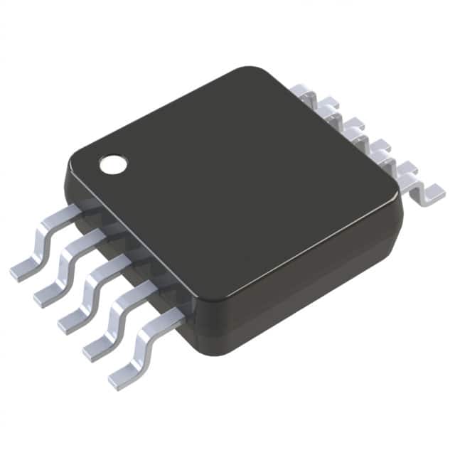
The AD5312BRM is offered in a 10-lead MSOP package and is designed for surface mount assembly. It is suitable for applications such as portable battery-powered instruments, digital gain and offset adjustment, and programmable voltage sources.
The AD5312BRM has a resolution of 10 bits.
The supply voltage range is 2.5V to 5.5V.
The operating temperature range is -40°C to 105°C.
The AD5312BRM is available in a 10-MSOP package.
The typical settling time is 9 µs.
The AD5312BRM supports SPI and DSP data interfaces.
The typical supply current is 300 µA at 5V.