

| Distributor | Stock | Pricing | MOQ | PKG | Lead Time | Date Code | On Order Quantity | On Order Delivery | |
|---|---|---|---|---|---|---|---|---|---|
|
964 pcs
|
964 pcs | On Request | 1 | On Request | On Request | On Request | On Request | On Request |
| Category | |
| Manufacturer Name | |
| Differential | |
| Frequency | |
| Input | |
| Lead Spacing | |
| Lead Style | |
| Main Purpose | |
| Mounting Type | |
| Number of Circuits | |
| Operating Temperature | |
| Output | |
| PLL | |
| Ratio | |
| Supplier Device Package | |
| Voltage |
The 9ZXL0853EKILF is an application-specific clock timing integrated circuit from Renesas, designed for Intel QPI and PCI Express (PCIe) applications. It provides a 1:12 input-to-output ratio with differential HCSL input and LP-HCSL outputs, supporting frequencies up to 400 MHz.
The device incorporates a phase-locked loop (PLL) with bypass capability, enabling both synthesized and direct clock distribution. It operates from a supply voltage of 3.135 V to 3.465 V and contains one clock distribution circuit. The differential input and output structure is suited for high-speed, low-noise clock distribution.
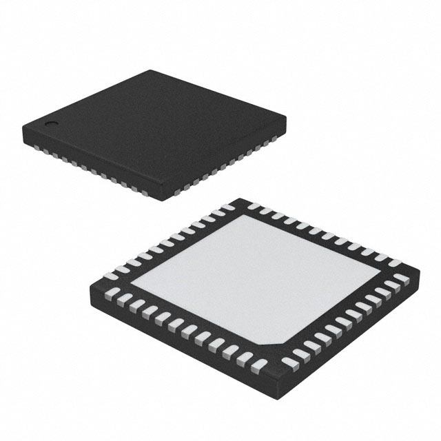
The 9ZXL0853EKILF is offered in a 48-VFQFPN (6x6 mm) package, also described as a 48-VFQFN exposed pad package, and is designed for surface-mount assembly. It operates over an ambient temperature range of -40°C to +85°C.
This clock timing IC is appropriate for systems needing clean clock generation and distribution for Intel QPI interconnects and PCI Express buses. The LP-HCSL output signaling provides low-power differential clocking for performance-sensitive applications.
The supply voltage range is 3.135 V to 3.465 V.
The device is available in a 48-VFQFPN (6x6 mm) package, described as a 48-VFQFN exposed pad package.
The operating temperature range is -40°C to +85°C (TA).
The product data lists the part as RoHS3 compliant.
The maximum frequency is 400 MHz.
The input-to-output ratio is 1:12.
It supports HCSL differential input and LP-HCSL differential output.