

| Distributor | Stock | Pricing | MOQ | PKG | Lead Time | Date Code | On Order Quantity | On Order Delivery | |
|---|---|---|---|---|---|---|---|---|---|
|
2,593 pcs
|
2593 pcs | On Request | 1 | On Request | On Request | On Request | On Request | On Request |
| Category | |
| Manufacturer Name | |
| Differential | |
| Divider | |
| Frequency | |
| Input | |
| Mounting Type | |
| Number of Circuits | |
| Operating Temperature | |
| Output | |
| PLL | |
| Ratio | |
| Supplier Device Package | |
| Tape & Reel | |
| Type | |
| Voltage |
The 9FGV1006CQ537LTGI8 is a clock generator IC from Renesas, designed with an integrated phase-locked loop (PLL) for flexible clock generation. It provides a 1:3 input-to-output ratio, accepting inputs from HCSL, LVCMOS, LVDS, or crystal sources, and delivering outputs in CML, HCSL, LP-HCSL, LVCMOS, LVDS, or LVPECL formats. The device supports both single-ended and differential output configurations.
Electrical specifications include three operating voltage ranges: 1.71V to 1.89V, 2.375V to 2.625V, and 3.135V to 3.465V, allowing compatibility with various logic levels. The maximum output frequency is 325MHz, with a secondary frequency of 200MHz. The IC operates over an industrial temperature range of -40°C to 85°C, making it suitable for demanding environments.
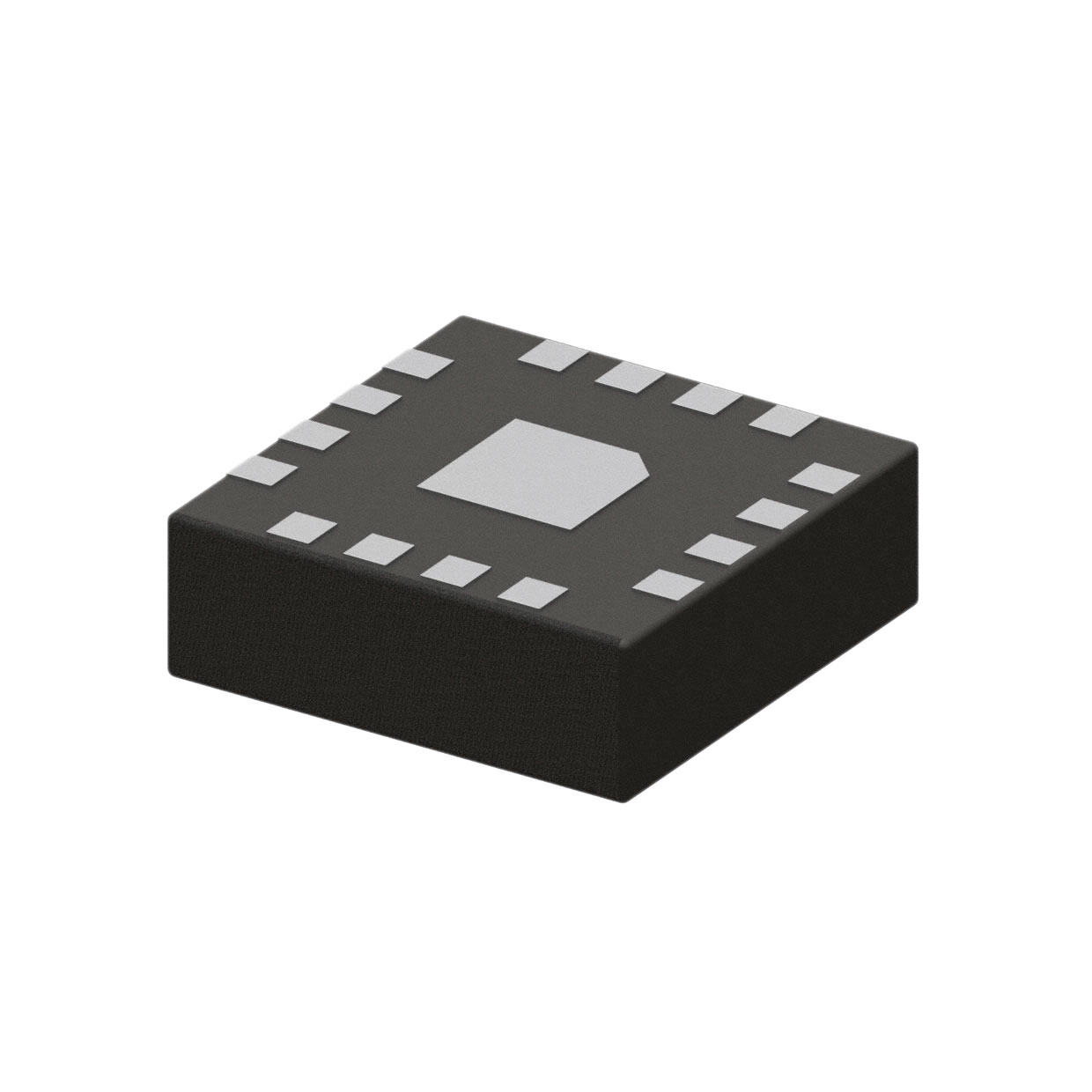
The device is packaged in a 16-TFLGA with exposed pad, surface-mount configuration, and the supplier device package is 16-LGA (3x3mm). This compact package is ideal for space-constrained designs. Compliance data indicates RoHS3 compliance, MSL 1 (unlimited floor life), and REACH unaffected status, though these have not been verified against a manufacturer datasheet.
1.71V to 1.89V, 2.375V to 2.625V, and 3.135V to 3.465V.
16-TFLGA Exposed Pad, 16-LGA (3x3) supplier package, surface mount.
-40°C to 85°C (TA).
RoHS3 Compliant (unverified).
200 MHz and 325 MHz.
HCSL, LVCMOS, LVDS, and Crystal.
1:3.