

| Distributor | Stock | Pricing | MOQ | PKG | Lead Time | Date Code | On Order Quantity | On Order Delivery | |
|---|---|---|---|---|---|---|---|---|---|
|
82 pcs
|
82 pcs | On Request | 1 | On Request | On Request | 24+ | On Request | On Request |
| Category | |
| Manufacturer Name | |
| Differential | |
| Frequency | |
| Input | |
| Input Type | |
| Lead Style | |
| Main Purpose | |
| Mounting Type | |
| Number of Circuits | |
| Operating Temperature | |
| Output | |
| PLL | |
| Ratio | |
| Supplier Device Package | |
| Supplier Package | |
| Supply Voltage | |
| Voltage |
The Renesas 9DBV0831AKILF is an application-specific clock buffer IC. It is designed to provide precise clock signals for high-speed interfaces such as Ethernet and PCI Express (PCIe). The device operates with a supply voltage range of 1.7V to 1.9V and supports a maximum frequency of 137.5MHz.
Featuring HCSL (High-Speed Current Steering Logic) for both input and output signals, the 9DBV0831AKILF ensures signal integrity in demanding environments. It offers a 1:8 ratio of input to output circuits, with differential input and output capabilities. The operating temperature range is -40°C to 85°C, making it suitable for various industrial applications.
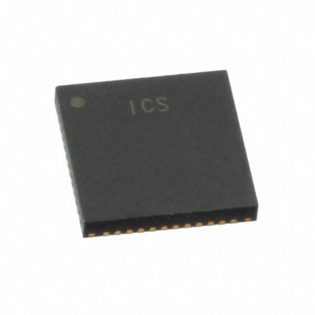
This clock buffer is available in a 48-VFQFN Exposed Pad package, designed for surface mounting. Its compact form factor and robust electrical characteristics make it a reliable choice for system designers requiring efficient clock distribution.
The maximum frequency for the 9DBV0831AKILF is 137.5MHz.
The 9DBV0831AKILF uses HCSL for both its input and output signals.
The operating supply voltage for this component is between 1.7V and 1.9V.
The device operates within a temperature range of -40°C to 85°C.
The 9DBV0831AKILF is supplied in a 48-VFQFN Exposed Pad package.
This clock buffer is designed for applications such as Ethernet and PCI Express (PCIe).