

| Distributor | Stock | Pricing | MOQ | PKG | Lead Time | Date Code | On Order Quantity | On Order Delivery | |
|---|---|---|---|---|---|---|---|---|---|
|
110 pcs
|
110 pcs | On Request | 1 | On Request | On Request | On Request | On Request | On Request |
| Category | |
| Manufacturer Name | |
| Differential | |
| Frequency | |
| Input | |
| Main Purpose | |
| Mounting Type | |
| Number of Circuits | |
| Operating Temperature | |
| Output | |
| PLL | |
| Ratio | |
| SVHC Present | |
| Supplier Device Package | |
| Voltage |
The 9DB833AGILFT is a Renesas clock buffer designed for PCI Express (PCIe) applications. It accepts one HCSL differential input and distributes it to eight HCSL differential outputs, providing a 1:8 fanout. The device includes an integrated PLL and supports a maximum output frequency of 166 MHz, making it suitable for PCIe Gen3 clock distribution in servers, switches, and other high-speed digital systems.
The buffer operates from a 3.3V supply (3.135V to 3.465V) and is specified for an ambient operating temperature range of -40°C to +85°C. All inputs and outputs use HCSL signaling, which is commonly used in PCIe reference clock trees. The single-circuit design is optimized for low-jitter clock distribution.
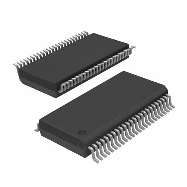
The device is offered in a 48-pin TFSOP package (6.10mm body width) with a 48-TSSOP supplier device package code. It is mounted using surface mount technology and is supplied on tape and reel. The part belongs to the 9DB833 series and is intended for PCIe clock buffering applications.
The supply voltage range is 3.135V to 3.465V (nominal 3.3V).
It is available in a 48-TFSOP package (0.240", 6.10mm width), also referred to as 48-TSSOP supplier device package, for surface mount.
-40°C to 85°C.
The part is listed as RoHS3 compliant, although this status is unverified and should be confirmed with the manufacturer.
166 MHz.
Both input and output are HCSL, and the device supports differential signaling.
It provides 8 outputs from a single input (1:8 fanout).