

| Distributor | Stock | Pricing | MOQ | PKG | Lead Time | Date Code | On Order Quantity | On Order Delivery | |
|---|---|---|---|---|---|---|---|---|---|
|
14,601 pcs
|
14601 pcs | On Request | 1 | On Request | On Request | On Request | On Request | On Request |
| Category | |
| Manufacturer Name | |
| Differential | |
| Frequency | |
| Halogen Free | |
| Input | |
| Main Purpose | |
| Mounting Type | |
| Number of Circuits | |
| Operating Temperature | |
| Output | |
| PLL | |
| Ratio | |
| SVHC Present | |
| Supplier Device Package | |
| Voltage |
The Renesas 9DB833AFILFT is an integrated circuit specifically designed as a clock fanout/buffer for PCI Express (PCIe) systems. This device supports a maximum frequency of 166MHz and operates with a supply voltage between 3.135V and 3.465V. It features HCSL (High-Current Source Logic) input and output, with a 1:8 ratio, indicating one input to eight outputs.
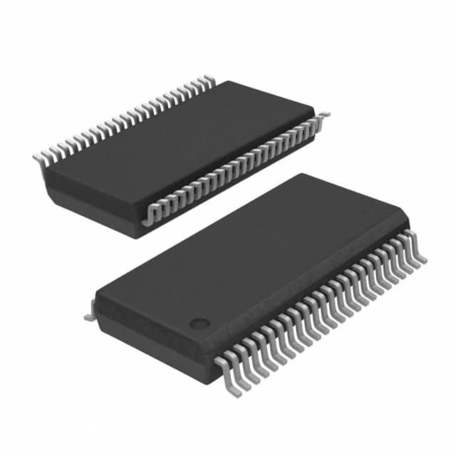
Packaged in a 48-SSOP (Supplier Device Package) or 48-BSSOP (0.295", 7.50mm Width) for surface mount applications, the 9DB833AFILFT is suitable for various board designs. It includes a Phase-Locked Loop (PLL) for precise clock generation and distribution. The operating temperature range of -40°C to 85°C ensures reliable performance in industrial and commercial environments.
This clock buffer is ideal for applications requiring robust clock signal integrity and distribution, particularly within PCIe architectures. Its differential Yes/Yes configuration further enhances signal quality and noise immunity.
The 9DB833AFILFT has a maximum operating frequency of 166MHz.
The 9DB833AFILFT operates within a voltage range of 3.135V to 3.465V.
The operating temperature range for the 9DB833AFILFT is -40°C to 85°C.
The 9DB833AFILFT is available in a 48-SSOP supplier device package and a 48-BSSOP (0.295", 7.50mm Width) package/case.
The 9DB833AFILFT uses Surface Mount technology for installation.
The 9DB833AFILFT is RoHS3 Compliant.
The Moisture Sensitivity Level (MSL) for the 9DB833AFILFT is 1 Unlimited.