

| Distributor | Stock | Pricing | MOQ | PKG | Lead Time | Date Code | On Order Quantity | On Order Delivery | |
|---|---|---|---|---|---|---|---|---|---|
|
8,107 pcs
|
8107 pcs | On Request | 1 | On Request | On Request | On Request | On Request | On Request |
| Category | |
| Manufacturer Name | |
| Input | |
| Main Purpose | |
| Mounting Type | |
| Number of Circuits | |
| Operating Temperature | |
| Output | |
| PLL | |
| Voltage Supply |
The 9DB823BGLF is an integrated circuit designed for clock generation and distribution, specifically for PC applications. Manufactured by Integrated Device Technology, this component operates within a supply voltage range of 3.135V to 3.465V and supports a maximum frequency of 400MHz.
Key electrical characteristics include a 1:9 input-to-output ratio and differential HCSL inputs and outputs, making it suitable for high-speed interfaces like Intel QPI and PCI Express (PCIe). The device incorporates a Phase-Locked Loop (PLL) for precise clock signal generation.
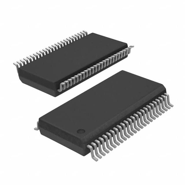
Packaged in a 48-TSSOP surface mount configuration, the 9DB823BGLF is designed for efficient board space utilization. It operates within a temperature range of 0°C to 70°C, ensuring reliable performance in typical operating environments. This component is intended for applications requiring stable and high-frequency clock signals.
| Qty | Low | High |
|---|---|---|
| 1+ | $0.99 | $0.99 |
Estimated market price range - modelled values for guidance only, not live distributor offers.
The operating voltage for the 9DB823BGLF is between 3.135V and 3.465V.
The maximum frequency for the 9DB823BGLF is 400MHz.
The 9DB823BGLF has a ratio of 1:9 for input to output.
The 9DB823BGLF operates within a temperature range of 0°C to 70°C.
The 9DB823BGLF is available in a 48-TSSOP package.
The main purpose of the 9DB823BGLF is for Intel QPI and PCI Express (PCIe) applications.