

| Distributor | Stock | Pricing | MOQ | PKG | Lead Time | Date Code | On Order Quantity | On Order Delivery | |
|---|---|---|---|---|---|---|---|---|---|
|
8,777 pcs
|
8777 pcs | On Request | 1 | On Request | On Request | On Request | On Request | On Request |
| Category | |
| Manufacturer Name | |
| Differential | |
| Frequency | |
| Input | |
| Main Purpose | |
| Mounting Type | |
| Number of Circuits | |
| Operating Temperature | |
| Output | |
| PLL | |
| Ratio | |
| Supplier Device Package | |
| Voltage |
The 9DB801CGLFT-INT is a single-circuit PLL-based clock generator IC from Renesas, designed specifically for PCI Express (PCIe) applications. It accepts an HCSL input and provides up to eight differential outputs in either HCSL or LVDS logic, with a maximum output frequency of 400 MHz. The device operates from a supply voltage of 3.135V to 3.465V and is specified over a temperature range of 0°C to 70°C.
This clock generator integrates a phase-locked loop (PLL) to generate low-jitter clocks suitable for high-speed serial interfaces. The 1:8 fanout ratio allows distribution of a single reference clock to multiple PCIe lanes or devices. The differential input and output architecture ensures signal integrity in noisy environments.
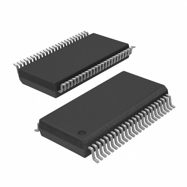
The IC is housed in a 48-TFSOP package (0.240", 6.10mm width), also referred to as 48-TSSOP, and is surface mount compatible. It is intended for use in computing, networking, and communications systems requiring PCIe clock generation.
3.135V to 3.465V.
48-TFSOP (0.240", 6.10mm Width) also known as 48-TSSOP.
0°C to 70°C.
RoHS3 Compliant (unverified).
HCSL.
HCSL and LVDS.
400 MHz.