

| Distributor | Stock | Pricing | MOQ | PKG | Lead Time | Date Code | On Order Quantity | On Order Delivery | |
|---|---|---|---|---|---|---|---|---|---|
|
10,696 pcs
|
10696 pcs | On Request | 1 | On Request | On Request | On Request | On Request | On Request |
| Category | |
| Manufacturer Name | |
| Input Type | |
| Main Purpose | |
| Mounting Type | |
| Number of Circuits | |
| Output Type | |
| PLL | |
| Supply Voltage |
The Renesas Electronics America Inc 9DB801BFLF is an application-specific clock buffer designed for PCI Express (PCIe) Gen1 applications. This component provides 8 outputs with HCSL and LVDS interfaces, supporting a maximum frequency of 400MHz. It operates within a supply voltage range of 3.135V to 3.465V and has an operating temperature range of 0°C to 70°C.
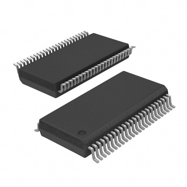
The 9DB801BFLF is housed in a 48-BSSOP surface mount package, measuring 7.50mm in width. Its input and output signals utilize HCSL and LVDS standards, respectively, with a ratio of 1:8 from input to output. The device is designed for applications requiring precise clock distribution in PCIe environments.
Environmental compliance includes RoHS3 compliance and an MSL 1 rating, indicating unlimited moisture sensitivity. The REACH status is unaffected. This clock buffer is suitable for various electronic designs where reliable clock signal generation and distribution are critical.
| Qty | Low | High |
|---|---|---|
| 1+ | $0.99 | $0.99 |
Estimated market price range - modelled values for guidance only, not live distributor offers.
The maximum frequency is 400MHz.
The input type is HCSL, and the output types are HCSL and LVDS.
The supply voltage range is 3.135V to 3.465V.
The operating temperature range is 0°C to 70°C.
It is in a 48-BSSOP package.
The main purpose is PCI Express (PCIe).