

| Distributor | Stock | Pricing | MOQ | PKG | Lead Time | Date Code | On Order Quantity | On Order Delivery | |
|---|---|---|---|---|---|---|---|---|---|
|
625 pcs
|
625 pcs | On Request | 1 | On Request | On Request | 08+ | On Request | On Request |
| Category | |
| Manufacturer Name | |
| Halogen Free | |
| Input Type | |
| Main Purpose | |
| Mounting Type | |
| Number of Circuits | |
| Operating Temperature | |
| Operating Voltage | |
| Output Type | |
| PLL | |
| SVHC Present | |
| Tape & Reel |
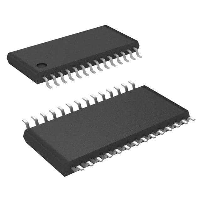
The 9DB403DFILF from Renesas Electronics America Inc is a specialized integrated circuit designed as a differential clock buffer. It features 4 outputs and is housed in a 28-TSSOP package, suitable for surface mount applications.
This component operates within a supply voltage range of 3.135V to 3.465V and can handle a maximum frequency of 400MHz. The input type is HCSL, and the outputs support HCSL and LVDS signaling. It is designed for applications such as PCI Express (PCIe).
The device is specified for an operating temperature range of 0°C to 70°C. Its RoHS status is compliant with RoHS3 standards. The packaging is provided in a tube, and it is designed for surface mounting.
| Qty | Low | High |
|---|---|---|
| 1+ | $2.01 | $2.01 |
Estimated market price range - modelled values for guidance only, not live distributor offers.
The operating voltage for the 9DB403DFILF is between 3.135V and 3.465V.
The 9DB403DFILF supports a maximum frequency of 400MHz.
The 9DB403DFILF is supplied in a 28-TSSOP package.
The operating temperature range for the 9DB403DFILF is 0°C to 70°C.
The output types for the 9DB403DFILF are HCSL and LVDS.
Yes, the 9DB403DFILF is RoHS3 Compliant.