

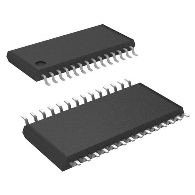
9DB401BGLFT The 9DB401BGLFT is a PCI Express clock buffer from Renesas. It features 1:4 differential outputs, HCSL/LVDS logic, and operates up to 333.33MHz.
Mfr Part #:

9DB401BGLFT

Available from 1 distributors
Mfr Name: Renesas
Renesas
The 9DB401BGLFT is a PCI Express clock buffer from Renesas. It features 1:4 differential outputs, HCSL/LVDS logic, and operates up to 333.33MHz.
Total Stock: 2,638 pcs

9DB401BGLFT Available from 1 distributor

Authorised
Non-Authorised
Distributor Stock Pricing MOQ PKG Lead Time Date Code On Order Quantity On Order Delivery
Non-Authorised Inventory information
2,638 pcs
2638 pcs On Request 1 On Request On Request On Request On Request On Request

9DB401BGLFT Specifications Quick View

Most important parameters for selection – full specs in datasheet.
Category
Manufacturer Name
Differential
Frequency
Input
Main Purpose
Mounting Type
Number of Circuits
Operating Temperature
Output
PLL
Ratio
Supplier Device Package
Voltage

9DB401BGLFT Description

Short technical summary and product information.

The Renesas 9DB401BGLFT is a 1:4 differential clock buffer designed for PCI Express applications. It accepts HCSL input signals and provides both HCSL and LVDS output logic, offering flexibility for interfacing with downstream devices.


The device operates from a supply voltage of 3.135V to 3.465V and can generate output frequencies up to 333.33 MHz. It includes a PLL for clock cleaning and supports a 1:4 input-to-output ratio with differential signaling on both input and output sides.


Housed in a 28-TSSOP package (0.173", 4.40mm width) with surface mount mounting, this buffer is suitable for space-constrained designs. The operating temperature range is 0°C to 70°C, making it appropriate for commercial and industrial environments.


This component is intended for clock distribution in PCIe-based systems such as servers, networking equipment, and data communication hardware.

9DB401BGLFT Quick Information

Product Type: PCI Express Clock Buffer
Canonical Name: Renesas 9DB401BGLFT PCI Express 1:4 Differential Clock Buffer
Subcategory: Application Specific Clock/Timing

9DB401BGLFT Compliance

RoHS Status: RoHS Compliant
Moisture Sensitivity Level (MSL): 1 Unlimited
REACH Status: REACH Unaffected

9DB401BGLFT Features

  • 1:4 differential clock buffer for PCIe.
  • Supports HCSL inputs and HCSL/LVDS outputs.
  • Maximum frequency of 333.33 MHz.
  • Supply voltage range 3.135V to 3.465V.
  • Operating temperature 0°C to 70°C.

9DB401BGLFT Applications

  • PCI Express clock distribution buffer
  • 1:4 differential clock fanout
  • HCSL-to-LVDS clock translation
  • High-frequency PCIe clock buffering
  • Surface-mount PCIe timing solution

9DB401BGLFT FAQs

7 frequently asked questions generated from this part’s specifications.
What is the operating voltage range of the 9DB401BGLFT?

3.135V to 3.465V.

What package is the 9DB401BGLFT available in?

28-TSSOP (0.173", 4.40mm Width).

What is the operating temperature range of the 9DB401BGLFT?

0°C to 70°C.

Is the 9DB401BGLFT RoHS compliant?

RoHS3 Compliant (unverified).

What is the maximum output frequency of the 9DB401BGLFT?

333.33 MHz.

What is the input to output ratio of the 9DB401BGLFT?

1:4.

What output logic types does the 9DB401BGLFT support?

HCSL and LVDS.

9DB401BGLFT Alternate Parts

Same form/fit/function or matching attribute configuration across different manufacturers.
View All Alternate Parts
9DB401BGLF
9DB401BGLF
Renesas
IC BUFFER 4OUTPUT DIFF 28-TSSOP
View Part
Home
Account

Categories