

| Distributor | Stock | Pricing | MOQ | PKG | Lead Time | Date Code | On Order Quantity | On Order Delivery | |
|---|---|---|---|---|---|---|---|---|---|
|
2,878 pcs
|
2878 pcs | On Request | 1 | On Request | On Request | On Request | On Request | On Request |
| Category | |
| Manufacturer Name | |
| Differential | |
| Frequency | |
| Input | |
| Main Purpose | |
| Mounting Type | |
| Number of Circuits | |
| Operating Temperature | |
| Output | |
| PLL | |
| Ratio | |
| Supplier Device Package | |
| Voltage |
The Renesas 9DB233AGLFT is an application-specific clock and timing device designed for PCI Express (PCIe) systems. It features an integrated phase-locked loop (PLL) and fanout buffer, accepting a clock input and distributing two HCSL differential output pairs. The device operates at a maximum frequency of 110 MHz and requires a supply voltage between 3.135V and 3.465V.
This zero delay buffer ensures precise synchronization and low jitter, making it suitable for PCIe reference clock generation. It supports a differential input and provides differential outputs, maintaining signal integrity across the system.
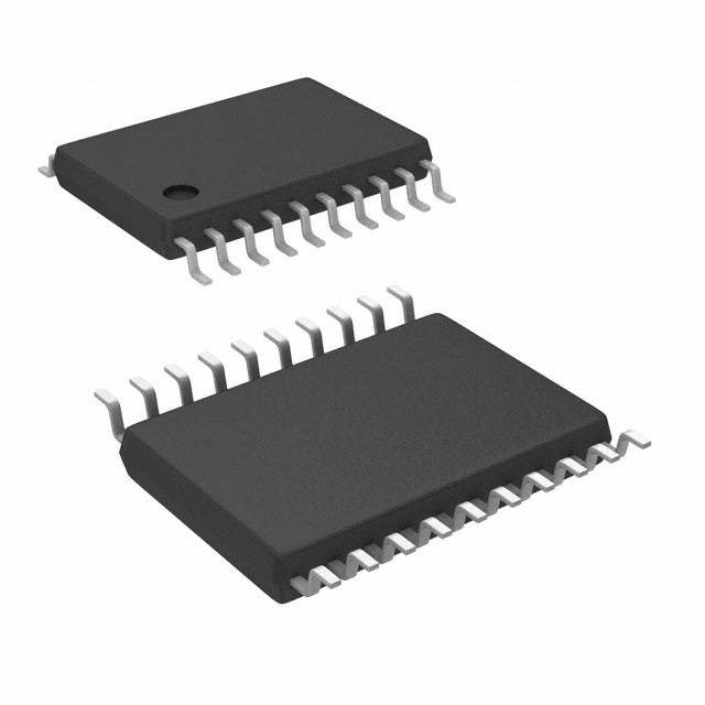
The IC is housed in a surface-mount 20-TSSOP package with a 4.40mm body width, designed for efficient PCB layout. It operates over a commercial temperature range of 0°C to 70°C, covering typical computing and networking environments.
With its 1:2 fanout ratio, the 9DB233AGLFT enables clock distribution to multiple PCIe endpoints without external components. Its small footprint and standard supply voltage simplify integration into existing designs.
The supply voltage range is 3.135V to 3.465V.
It comes in a 20-TSSOP package with dimensions 0.173" (4.40mm Width).
The operating temperature range is 0°C to 70°C.
According to existing data, it is marked as ROHS3 Compliant, but this has not been independently verified.
It provides HCSL (High-Speed Current Steering Logic) differential outputs.
It has a 1:2 input-to-output ratio, meaning two outputs for one input.
The maximum frequency is 110 MHz.