


| Distributor | Stock | Pricing | MOQ | PKG | Lead Time | Date Code | On Order Quantity | On Order Delivery | |
|---|---|---|---|---|---|---|---|---|---|
|
2,568 pcs
|
2568 pcs | On Request | 1 | On Request | On Request | On Request | On Request | On Request |
| Category | |
| Manufacturer Name | |
| Differential | |
| Frequency | |
| Input | |
| Main Purpose | |
| Mounting Type | |
| Number of Circuits | |
| Operating Temperature | |
| Output | |
| PLL | |
| Ratio | |
| Supplier Device Package | |
| Voltage |
The Renesas 9DB1200CGLFT is an Application Specific Clock/Timing IC designed for clock buffering applications. It features a 1:12 input to output ratio and supports a maximum frequency of 400MHz. The device operates within a voltage supply range of 3.135V to 3.465V and has an operating temperature range of 0°C to 70°C.
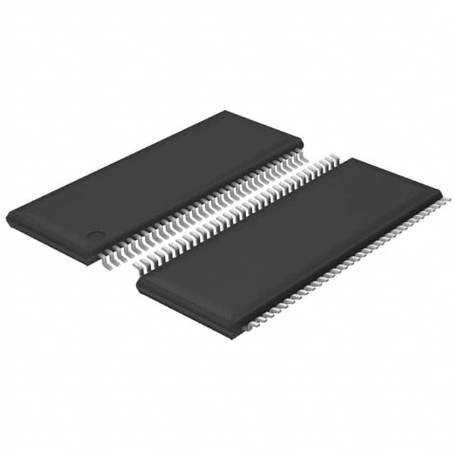
This IC is primarily intended for PCI Express (PCIe) applications, utilizing HCSL output and Clock input. It includes a PLL (Phase-Locked Loop) and contains one circuit. The component is provided in a 64-TFSOP (0.240", 6.10mm Width) package, with a supplier device package of 64-TSSOP, and is designed for surface mount applications.
The maximum operating frequency of the 9DB1200CGLFT is 400MHz.
The operating temperature range for the 9DB1200CGLFT is 0°C to 70°C.
The 9DB1200CGLFT is available in a 64-TFSOP (0.240", 6.10mm Width) package.
The supply voltage range for the 9DB1200CGLFT is 3.135V to 3.465V.
The input to output ratio of this clock buffer is 1:12.
The mounting type for the 9DB1200CGLFT is Surface Mount.
The 9DB1200CGLFT is RoHS3 Compliant.