

| Distributor | Stock | Pricing | MOQ | PKG | Lead Time | Date Code | On Order Quantity | On Order Delivery | |
|---|---|---|---|---|---|---|---|---|---|
|
461 pcs
|
461 pcs | On Request | 1 | On Request | On Request | On Request | On Request | On Request |
| Category | |
| Manufacturer Name | |
| Differential | |
| Frequency | |
| Input | |
| Input Type | |
| Main Purpose | |
| Mounting Type | |
| Number of Circuits | |
| Operating Mode | |
| Operating Temperature | |
| Output | |
| PLL | |
| Ratio | |
| Supplier Device Package | |
| Voltage |
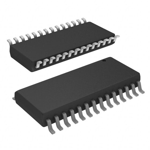
The 9DB104BFLFT from Renesas is an Application Specific ClockTiming Integrated Circuit, specifically configured as a 1:4 ratio clock buffer. This device is primarily intended for PCI Express (PCIe) applications, ensuring precise clock signal distribution. It operates efficiently within a supply voltage range of 3.135V to 3.465V and can handle frequencies up to 220MHz.
This IC features a single circuit with differential inputs and outputs, supporting both clock input and output types. It includes a Phase-Locked Loop (PLL) for stable clock generation and distribution. The device is designed for surface mount applications and comes in a 28-SSOP package, measuring 0.209 inches (5.30mm) in width. Its operating temperature range is from 0°C to 70°C, making it suitable for various commercial and industrial environments.
The 9DB104BFLFT operates within a temperature range of 0°C to 70°C.
The 9DB104BFLFT is supplied in a 28-SSOP (0.209", 5.30mm Width) package.
The 9DB104BFLFT operates with a supply voltage ranging from 3.135V to 3.465V.
The 9DB104BFLFT supports a frequency of 220MHz.
The output cycle-cycle jitter is less than 50ps.
The output skew is less than 50ps.
Yes, it is tolerant to spread spectrum modulation from 0 to -0.5% down spread and +/- 0.25% center spread.