

| Distributor | Stock | Pricing | MOQ | PKG | Lead Time | Date Code | On Order Quantity | On Order Delivery | |
|---|---|---|---|---|---|---|---|---|---|
|
160 pcs
|
160 pcs | On Request | 1 | On Request | On Request | 21+ | On Request | On Request |
| Category | |
| Manufacturer Name | |
| Differential | |
| Divider | |
| Frequency | |
| Input | |
| Mounting Type | |
| Number of Circuits | |
| Operating Temperature | |
| Output | |
| PLL | |
| Ratio | |
| SVHC Present | |
| Supplier Device Package | |
| Type | |
| Voltage |
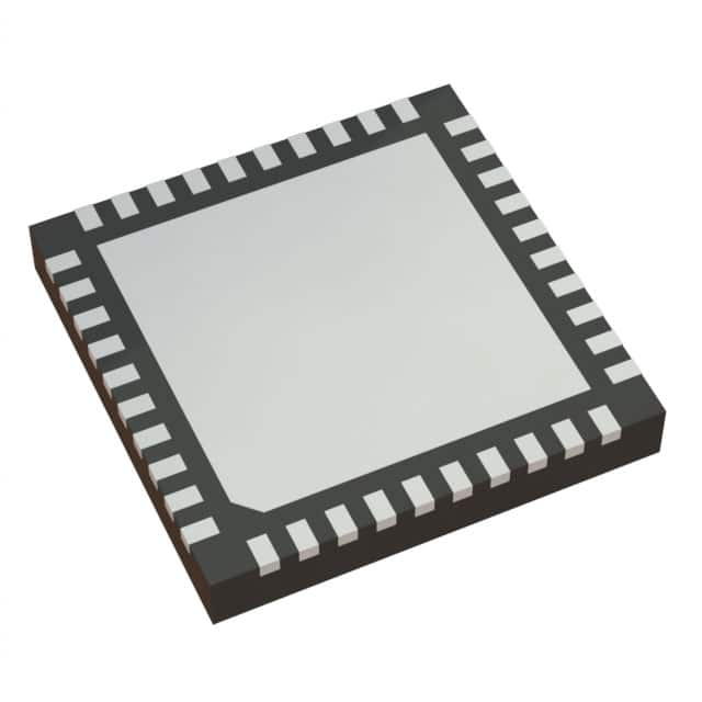
The Renesas 8T49N241-998NLGI is a high-performance Frequency Translator and Jitter Attenuator integrated circuit. It incorporates a PLL with bypass mode, enabling flexible frequency synthesis and jitter cleaning for complex clocking requirements.
The device supports a wide variety of input logic types including LVCMOS, LVDS, LVHSTL, LVPECL, and Crystal, and provides configurable outputs in HCSL, LVCMOS, LVDS, and LVPECL formats. With a maximum operating frequency of 1 GHz and a 3:4 input-to-output ratio, it is well-suited for translating and distributing high-speed clocks in communication systems.
The IC operates over a supply voltage range of 2.375V to 3.465V and an industrial temperature range of -40°C to 85°C. It is housed in a 40-VFQFN exposed pad package (supplier package 40-VFQFPN 6x6 mm) and is designed for surface mount assembly. The FemtoClock NG series offers low jitter performance for demanding timing applications.
2.375V to 3.465V
40-VFQFN Exposed Pad (supplier package 40-VFQFPN 6x6 mm)
-40°C to 85°C
Unverified data indicates RoHS3 Compliant. Confirm with official documentation.
1 GHz
LVCMOS, LVDS, LVHSTL, LVPECL, Crystal
Yes, with bypass mode.