

| Distributor | Stock | Pricing | MOQ | PKG | Lead Time | Date Code | On Order Quantity | On Order Delivery | |
|---|---|---|---|---|---|---|---|---|---|
|
124 pcs
|
124 pcs | On Request | 1 | On Request | On Request | On Request | On Request | On Request |
| Category | |
| Manufacturer Name | |
| Differential | |
| Frequency | |
| Industrial Grade | |
| Input | |
| Mounting Type | |
| Number of Circuits | |
| Operating Temperature | |
| Output | |
| Ratio | |
| SVHC Present | |
| Supplier Device Package | |
| Type | |
| Voltage |
The 8SLVP2104ANBGI/W is a clock fanout buffer (distribution) IC from Renesas Electronics Corporation. It provides two circuits each with a 1:4 input-to-output ratio, supporting differential inputs and outputs. The device accepts CML, LVCMOS, LVDS, and LVPECL input signals and outputs LVPECL.
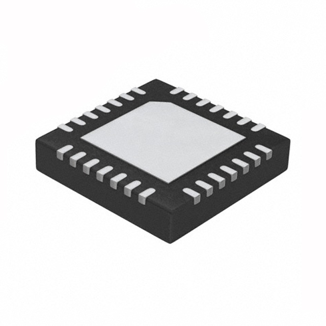
Operating from a supply voltage of 2.375V to 3.465V, the IC achieves a maximum frequency of 2 GHz. It is designed for surface mount assembly in a 28-WFQFN exposed pad package (supplier device package 28-VFQFPN 5x5 mm). The operating temperature range is -40°C to 85°C.
This fanout buffer is suitable for clock distribution in high-speed digital systems requiring multiple low-jitter clock outputs. The differential signaling support makes it appropriate for applications where signal integrity over long traces or between boards is critical.
The maximum frequency is 2 GHz.
The supply voltage range is 2.375V to 3.465V.
It comes in a 28-WFQFN exposed pad package (supplier device package 28-VFQFPN 5x5 mm).
The operating temperature range is -40°C to 85°C.
The output is LVPECL.
The device accepts CML, LVCMOS, LVDS, and LVPECL inputs.
RoHS status is listed as RoHS3 Compliant, but this is unverified low-confidence data.