

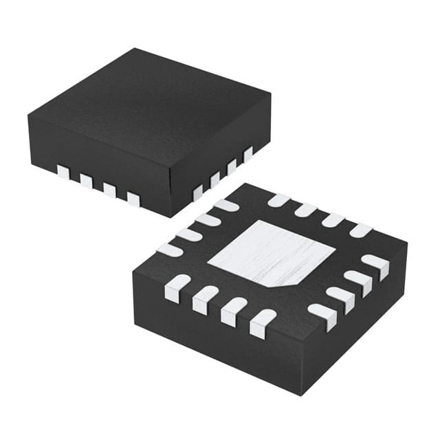
8SLVP2102ANLGI/W Renesas 8SLVP2102ANLGI/W is a high-speed clock fanout buffer with 1:2 input-to-output ratio. It operates at up to 2 GHz with LVPECL output and supports CML, LVDS, LVPECL inputs.
Mfr Part #:

8SLVP2102ANLGI/W

Available from 1 distributors
Mfr Name: Renesas
Renesas
Renesas 8SLVP2102ANLGI/W is a high-speed clock fanout buffer with 1:2 input-to-output ratio. It operates at up to 2 GHz with LVPECL output and supports CML, LVDS, LVPECL inputs.
✓ Total Stock: 90 pcs

8SLVP2102ANLGI/W Available from 1 distributor

✓ Authorised
✓ Non-Authorised
Distributor Stock Pricing MOQ PKG Lead Time Date Code On Order Quantity On Order Delivery
Non-Authorised Inventory information
90 pcs
90 pcs On Request 1 On Request On Request On Request On Request On Request

8SLVP2102ANLGI/W Specifications Quick View

Most important parameters for selection – full specs in datasheet.
Category
Manufacturer Name
Differential
Frequency
Input
Mounting Type
Number of Circuits
Operating Temperature
Output
Ratio
SVHC Present
Supplier Device Package
Type
Voltage

8SLVP2102ANLGI/W Description

Short technical summary and product information.

The Renesas 8SLVP2102ANLGI/W is a fanout buffer (distribution) integrated circuit designed for high-speed clock distribution. It provides two differential LVPECL outputs from a single differential input, supporting input signal types CML, LVDS, and LVPECL. The device operates over a wide supply voltage range of 2.375V to 3.465V and can handle clock frequencies up to 2 GHz. It is housed in a compact 16-VFQFN exposed pad package with dimensions 3x3 mm, suitable for surface mount assembly. The device is specified for an operating temperature range of -40°C to 85°C, making it suitable for industrial and commercial environments. The low jitter and low skew characteristics of this buffer ensure reliable clock distribution in high-speed digital systems. Typical applications include telecom, networking, data centers, and test equipment where precise timing is critical. The differential input/output capability helps maintain signal integrity over long traces. The exposed pad enhances thermal performance and electrical grounding.

8SLVP2102ANLGI/W Quick Information

Product Type: Clock Buffer, Fanout Buffer (Distribution)
Canonical Name: Renesas 8SLVP2102ANLGI/W Fanout Buffer (Distribution) 1:2 2GHz LVPECL Surface Mount
Subcategory: Fanout Buffer (Distribution)

8SLVP2102ANLGI/W Compliance

RoHS Status: RoHS Compliant
Moisture Sensitivity Level (MSL): 1 Unlimited
REACH Status: REACH Unaffected

8SLVP2102ANLGI/W Features

  • 1:2 differential fanout buffer with LVPECL outputs.
  • Supports input types CML, LVDS, LVPECL.
  • Maximum frequency of 2 GHz.
  • Supply voltage range 2.375V to 3.465V.
  • Industrial temperature range -40°C to 85°C.

8SLVP2102ANLGI/W Applications

  • Clock distribution in telecom equipment.
  • High-speed data center timing systems.
  • Test and measurement instrumentation.
  • Networking switches and routers.

8SLVP2102ANLGI/W FAQs

7 frequently asked questions generated from this part’s specifications.
What is the operating voltage range of the 8SLVP2102ANLGI/W?

2.375V to 3.465V.

What is the package type for this device?

16-VFQFN Exposed Pad (3x3mm).

What is the operating temperature range?

-40°C to 85°C.

Is the 8SLVP2102ANLGI/W RoHS compliant?

The product data indicates RoHS3 compliance and REACH unaffected, but this is unverified and has low confidence.

What is the maximum frequency the 8SLVP2102ANLGI/W can handle?

2 GHz.

What input signal types does the 8SLVP2102ANLGI/W support?

CML, LVDS, and LVPECL.

How many circuits does the 8SLVP2102ANLGI/W contain?

2 circuits.

Home
Account

Categories