

| Distributor | Stock | Pricing | MOQ | PKG | Lead Time | Date Code | On Order Quantity | On Order Delivery | |
|---|---|---|---|---|---|---|---|---|---|
|
10,000 pcs
|
10000 pcs | On Request | 1 | On Request | On Request | On Request | On Request | On Request |
| Category | |
| Manufacturer Name | |
| AEC Qualified | |
| Automotive Grade | |
| Differential | |
| Frequency | |
| Industrial Grade | |
| Medical Grade | |
| Military Grade | |
| Mounting Type | |
| Number of Circuits | |
| Operating Temperature | |
| Storage Temperature | |
| Supply Voltage | |
| Tape & Reel |
The 8SLVP1102ANLGI/W is a high-speed clock fanout buffer and multiplexer IC manufactured by Integrated Device Technology. It supports two differential clock inputs and provides eight outputs. This component operates within a supply voltage range of 2.375V to 3.465V and has a maximum frequency of 2 GHz, ensuring fast and stable clock distribution.
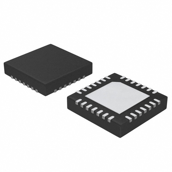
The device is designed for low jitter and low skew, making it reliable for timing-critical applications. It features a compact 28-VFQFPN package suitable for space-limited designs. The operating temperature range is -40°C to 85°C.
Key specifications include a 2:8 input to output ratio, CML, LVDS, and LVPECL input signal types, and LVPECL output signal type. The IC utilizes surface mount technology for stable installation.
This clock buffer is suitable for applications requiring precise clock signal distribution and management.
| Qty | Low | High |
|---|---|---|
| 1+ | $1.87 | $1.87 |
Estimated market price range - modelled values for guidance only, not live distributor offers.
The supply voltage range is 2.375V to 3.465V.
The maximum operating frequency is 2 GHz.
The operating temperature range is -40°C to 85°C.
The package is 28-VFQFPN (6x6).
It is a surface mount device.
Input signal types are CML, LVDS, and LVPECL. The output signal type is LVPECL.