

| Distributor | Stock | Pricing | MOQ | PKG | Lead Time | Date Code | On Order Quantity | On Order Delivery | |
|---|---|---|---|---|---|---|---|---|---|
|
5,634 pcs
|
5634 pcs | On Request | 1 | On Request | On Request | On Request | On Request | On Request |
| Category | |
| Manufacturer Name | |
| Differential | |
| Divider | |
| Frequency | |
| Input | |
| Mounting Type | |
| Number of Circuits | |
| Operating Temperature | |
| Output | |
| PLL | |
| Ratio | |
| Supplier Device Package | |
| Type | |
| Voltage |
The Renesas 8752CYLFT is a clock multiplier and zero delay buffer integrated circuit designed for clock distribution and frequency synthesis applications. It accepts LVCMOS or LVTTL input signals and provides LVCMOS or LVTTL outputs, supporting a maximum frequency of 240MHz.
The device features a 2:8 input-to-output ratio, allowing it to distribute one or two input clocks to eight outputs with minimal skew. It includes an integrated PLL with bypass capability, enabling flexible clock generation and jitter cleaning. The part also incorporates input and output dividers for frequency scaling.
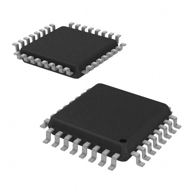
Housed in a 32-LQFP package with a 32-TQFP (7x7mm) supplier device package, the 8752CYLFT is designed for surface mount assembly. It operates over a commercial temperature range of 0°C to 70°C and supports a wide supply voltage range from 2.375V to 3.465V, making it suitable for various low-voltage digital systems.
The maximum frequency is 240MHz.
The supply voltage range is 2.375V to 3.465V.
It comes in a 32-LQFP package with a supplier device package of 32-TQFP (7x7mm).
The operating temperature range is 0°C to 70°C.
It is listed as RoHS3 Compliant, but this is unverified.
Both input and output logic are LVCMOS and LVTTL.
Yes, it has a PLL with bypass capability.