

| Distributor | Stock | Pricing | MOQ | PKG | Lead Time | Date Code | On Order Quantity | On Order Delivery | |
|---|---|---|---|---|---|---|---|---|---|
|
34,819 pcs
|
34819 pcs | On Request | 1 | On Request | On Request | On Request | On Request | On Request |
| Category | |
| Manufacturer Name | |
| Differential | |
| Frequency | |
| Input | |
| Main Purpose | |
| Mounting Type | |
| Number of Circuits | |
| Operating Temperature | |
| Output | |
| PLL | |
| Ratio | |
| Supplier Device Package | |
| Voltage |
The Renesas 874003BG-05LF is a PCI Express (PCIe) application specific clock/timing IC designed for jitter attenuation and fanout buffering. It integrates a PLL and provides a 1:3 input-to-output ratio with differential LVDS outputs. The device accepts a wide range of input logic standards including HCSL, LVDS, LVHSTL, LVPECL, and SSTL, making it versatile for various clock distribution architectures.
Operating from a supply voltage of 3.135V to 3.465V, the IC can handle input frequencies up to 320 MHz. It is a single-circuit device with both differential inputs and outputs, ensuring signal integrity in high-speed designs. The operating temperature range is 0°C to 70°C, suitable for commercial environments.
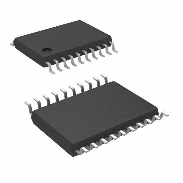
The part is housed in a surface-mount 20-pin TSSOP package (0.173" width, 4.40mm pitch) with supplier device package 20-TSSOP. This compact package is ideal for space-constrained PCB layouts in networking, server, and communication equipment requiring low-jitter PCI Express clock distribution.
The supply voltage range is 3.135V to 3.465V.
It is available in a surface mount 20-TSSOP package (0.173", 4.40mm width).
The operating temperature range is 0°C to 70°C.
It is listed as RoHS3 Compliant, but this status is unverified and should be confirmed from official documentation.
The maximum frequency is 320 MHz.
It has a 1:3 input-to-output ratio, providing three outputs.
It supports HCSL, LVDS, LVHSTL, LVPECL, and SSTL input logic.