

| Distributor | Stock | Pricing | MOQ | PKG | Lead Time | Date Code | On Order Quantity | On Order Delivery | |
|---|---|---|---|---|---|---|---|---|---|
|
8,372 pcs
|
8372 pcs | On Request | 1 | On Request | On Request | On Request | On Request | On Request |
| Category | |
| Manufacturer Name | |
| Differential | |
| Divider | |
| Frequency | |
| Input | |
| Mounting Type | |
| Number of Circuits | |
| Operating Temperature | |
| Output | |
| PLL | |
| Ratio | |
| SVHC Present | |
| Supplier Device Package | |
| Type | |
| Voltage |
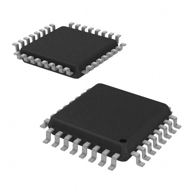
The ICS8705 (part number 8705BYLFT) is a high-performance differential-to-LVCMOS/LVTTL clock generator from Renesas, part of the HiPerClockS family. It integrates a fully programmable PLL and provides eight LVCMOS/LVTTL outputs with typical 7Ω output impedance. The device accepts differential input signals such as LVPECL, LVDS, LVHSTL, HCSL, and SSTL, as well as single-ended LVCMOS/LVTTL on the CLK0 input. It supports an input and output frequency range from 15.625 MHz to 250 MHz, with a VCO range of 250 MHz to 500 MHz.
The 8705BYLFT can be configured as a zero delay buffer, multiplier, or divider, with programmable dividers allowing output-to-input frequency ratios of 8:1, 4:1, 2:1, 1:1, 1:2, 1:4, and 1:8. The PLL can be bypassed for system test and debug. Key timing characteristics include cycle-to-cycle jitter of 45 ps maximum, output skew of 65 ps for CLK0 and 55 ps for CLK1/nCLK1, and static phase offset of 25 ±125 ps.
The device operates from a supply voltage of 2.375V to 3.465V and is specified over a commercial temperature range of 0°C to 70°C. It is housed in a 32-LQFP package with a 32-TQFP (7x7 mm) supplier package. This clock generator is ideal for applications requiring precise clock distribution with low jitter and flexible frequency synthesis.
2.375V to 3.465V.
32-LQFP (32-TQFP 7x7 mm).
0°C to 70°C.
Yes, it is RoHS3 compliant and lead free.
250 MHz.
HCSL, LVCMOS, LVDS, LVHSTL, LVPECL, LVTTL, SSTL.
45 ps maximum.