

| Distributor | Stock | Pricing | MOQ | PKG | Lead Time | Date Code | On Order Quantity | On Order Delivery | |
|---|---|---|---|---|---|---|---|---|---|
|
5,410 pcs
|
5410 pcs | On Request | 1 | On Request | On Request | On Request | On Request | On Request | |
|
1,660 pcs
|
1660 pcs | On Request | 1 | On Request | On Request | On Request | On Request | On Request |
| Category | |
| Manufacturer Name | |
| Differential | |
| Divider | |
| Frequency | |
| Input | |
| Mounting Type | |
| Number of Circuits | |
| Operating Temperature | |
| Output | |
| PLL | |
| Ratio | |
| SVHC Present | |
| Supplier Device Package | |
| Type | |
| Voltage |
The Renesas 87004AGLFT is a versatile clock timing IC that combines clock generation, zero delay buffering, fanout distribution, and multiplexing functions in a single device. It features one integrated circuit with a PLL that includes a bypass option, and provides a 2:4 input-to-output ratio with dividers.
The device accepts a wide range of differential input standards: HCSL, LVDS, LVHSTL, LVPECL, and SSTL. It outputs LVCMOS and LVTTL signals. The operating frequency reaches up to 250 MHz, making it suitable for high-speed clock distribution. The IC operates from a supply voltage range of 2.375V to 3.465V.
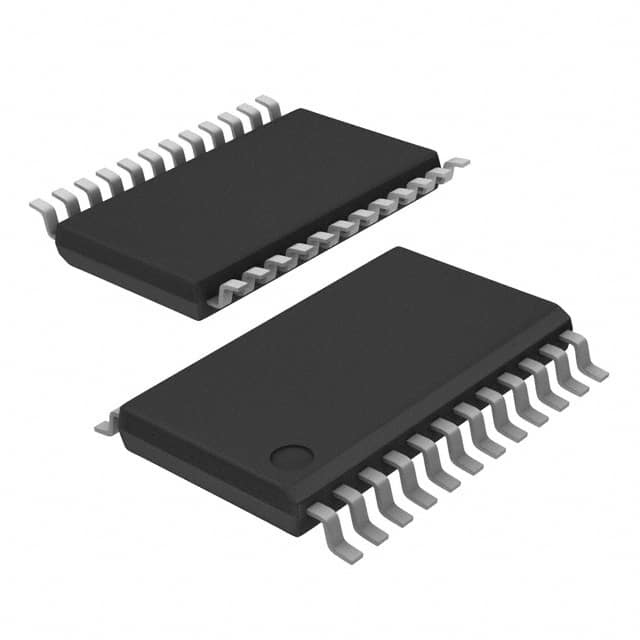
Packaged in a 24-TSSOP (0.173", 4.40mm Width) surface mount package, the 87004AGLFT is designed for standard surface mount assembly. Its operating temperature range is 0°C to 70°C, covering typical commercial applications.
This device is ideal for applications requiring precise clock distribution and zero delay buffering, such as networking equipment, telecommunications, and high-speed digital systems. The combination of multiple input types and programmable features provides design flexibility.
2.375V to 3.465V.
24-TSSOP (0.173", 4.40mm Width).
0°C to 70°C.
Yes, it is listed as RoHS3 compliant. (Note: unverified, low confidence).
250 MHz.
HCSL, LVDS, LVHSTL, LVPECL, SSTL.
Yes, with bypass.