

| Distributor | Stock | Pricing | MOQ | PKG | Lead Time | Date Code | On Order Quantity | On Order Delivery | |
|---|---|---|---|---|---|---|---|---|---|
|
4,506 pcs
|
4506 pcs | On Request | 1 | On Request | On Request | On Request | On Request | On Request |
| Category | |
| Manufacturer Name | |
| Differential | |
| Frequency | |
| Input | |
| Mounting Type | |
| Number of Circuits | |
| Operating Temperature | |
| Output | |
| Ratio | |
| SVHC Present | |
| Supplier Device Package | |
| Type | |
| Voltage |
The 8545BGLF is a clock buffer and fanout distribution IC from Renesas. It features a 2:4 fanout ratio, meaning it can accept two input clock signals and distribute them to four outputs. The device supports LVCMOS and LVTTL input levels and provides LVDS output signals, making it suitable for low-voltage differential signaling applications.
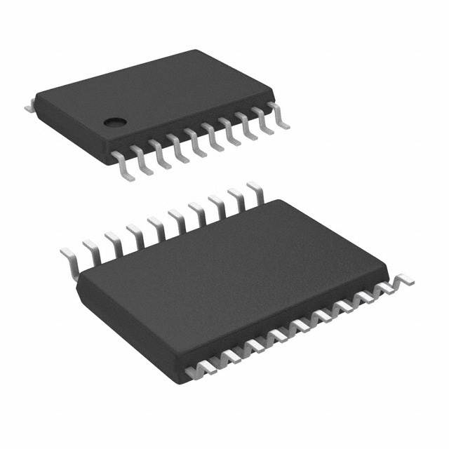
The buffer operates at a maximum frequency of 650 MHz and requires a supply voltage between 3.135V and 3.465V. It is designed for surface mount assembly in a 20-TSSOP package with a 4.40mm width. The operating temperature range is 0°C to 70°C.
This component is commonly used in clock distribution networks where low skew and high frequency are required. The LVDS outputs help reduce electromagnetic interference and support high-speed data transmission. The single circuit design provides a simple fanout solution for clock signals.
3.135V to 3.465V.
20-TSSOP (0.173", 4.40mm Width) surface mount package.
0°C to 70°C.
RoHS3 Compliant (unverified).
650 MHz.
2:4 (two inputs to four outputs).
Input: LVCMOS, LVTTL; Output: LVDS.