

| Distributor | Stock | Pricing | MOQ | PKG | Lead Time | Date Code | On Order Quantity | On Order Delivery | |
|---|---|---|---|---|---|---|---|---|---|
|
48,000 pcs
|
48000 pcs | On Request | 1 | On Request | On Request | On Request | On Request | On Request |
| Category | |
| Manufacturer Name | |
| Differential | |
| Frequency | |
| Input | |
| Mounting Type | |
| Number of Circuits | |
| Operating Temperature | |
| Output | |
| Ratio | |
| Supplier Device Package | |
| Type | |
| Voltage |
The 8545BGILF is a high-performance clock buffer and multiplexer from Renesas, designed to distribute clock signals with low jitter. It accepts two single-ended input channels (LVCMOS or LVTTL) and provides four LVDS output pairs, operating at frequencies up to 650 MHz. The device features a 2:4 ratio, allowing flexible clock routing and fanout.
The buffer operates from a 3.3V supply voltage (3.135V to 3.465V) and is specified over the industrial temperature range of -40°C to 85°C. Its differential outputs are ideal for driving high-speed digital loads in communication systems, networking equipment, and data centers.
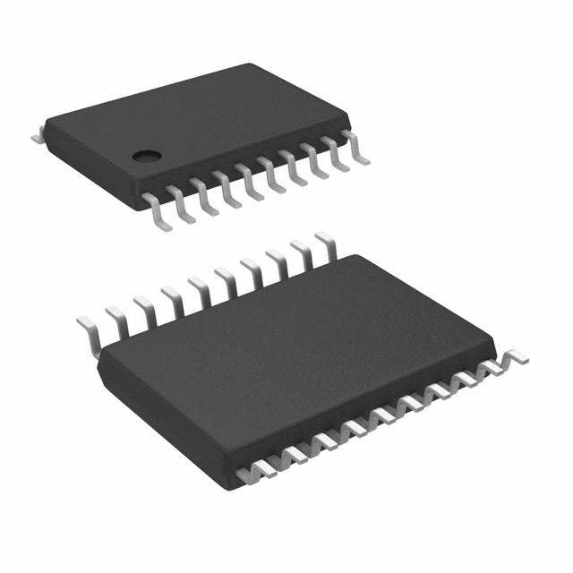
The 8545BGILF is housed in a 20-lead TSSOP package (4.40mm width), suitable for surface-mount assembly. The package is compact and compatible with standard PCB layouts. While the device is marked as RoHS3 compliant and REACH unaffected, these compliance statuses are unverified and should be confirmed with the manufacturer.
The supply voltage range is 3.135V to 3.465V.
It is available in a 20-TSSOP package (0.173", 4.40mm Width).
The operating temperature range is -40°C to 85°C.
It is listed as RoHS3 Compliant, but this is unverified and should be confirmed with the manufacturer.
Inputs: LVCMOS, LVTTL. Outputs: LVDS.
The maximum frequency is 650 MHz.
The ratio is 2:4 (two inputs, four outputs).