
853S111BYILFT
Renesas
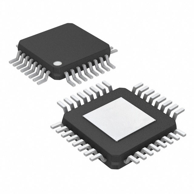
The 853S111BYILFT is a 2:10 fanout buffer and multiplexer from Renesas. It supports LVDS, LVPECL, and SSTL inputs, delivers ECL/LVPECL outputs at up to 2.5GHz, and comes in a 32-PTQFP-EP package.


| Distributor | Stock | Pricing | MOQ | PKG | Lead Time | Date Code | On Order Quantity | On Order Delivery | |
|---|---|---|---|---|---|---|---|---|---|
|
5,872 pcs
|
5872 pcs | On Request | 1 | On Request | On Request | On Request | On Request | On Request |
| Category | |
| Manufacturer Name | |
| Differential | |
| Frequency | |
| Input | |
| Mounting Type | |
| Number of Circuits | |
| Operating Temperature | |
| Output | |
| Ratio | |
| Supplier Device Package | |
| Type | |
| Voltage |
The 853S111BYILF is a clock fanout buffer and multiplexer IC manufactured by Renesas Electronics Corporation. It is designed for distribution of high-speed clock signals with a 2:10 input-to-output ratio, supporting differential inputs (LVDS, LVPECL, SSTL) and differential outputs (ECL, LVPECL). The device operates at a maximum frequency of 2.5 GHz and requires a supply voltage range of 2.375V to 3.8V.
This IC is suitable for applications requiring multiple clock outputs from a single or dual input sources, with the ability to select between two inputs. The device is housed in a 32-TQFP Exposed Pad package (32-PTQFP-EP, 7x7 mm) and is surface mountable. It operates over an industrial temperature range of -40°C to 85°C.
The combination of high frequency operation and differential signaling makes it ideal for use in telecommunications, networking, and data center equipment where low jitter and precise clock distribution are critical. The integrated multiplexer functionality allows for redundant clock source selection, enhancing system reliability.
The supply voltage range is 2.375V to 3.8V.
The device is available in a 32-TQFP Exposed Pad package (32-PTQFP-EP, 7x7 mm).
The operating temperature range is -40°C to 85°C.
It is listed as RoHS3 compliant (unverified).
The maximum frequency is 2.5 GHz.
The ratio is 2:10.
Inputs: LVDS, LVPECL, SSTL; Outputs: ECL, LVPECL.