

| Distributor | Stock | Pricing | MOQ | PKG | Lead Time | Date Code | On Order Quantity | On Order Delivery | |
|---|---|---|---|---|---|---|---|---|---|
|
2,349 pcs
|
2349 pcs | On Request | 1 | On Request | On Request | On Request | On Request | On Request |
| Category | |
| Manufacturer Name | |
| Differential | |
| Differential Output | |
| Divider | |
| Frequency | |
| Input | |
| Mounting Type | |
| Number of Circuits | |
| Operating Temperature | |
| Output | |
| PLL | |
| Ratio | |
| Supplier Device Package | |
| Type | |
| Voltage |
The 849S625BYILF is a clock synthesizer integrated circuit from Renesas Electronics Corporation. It is designed to generate clock signals for a variety of applications. The device incorporates a phase-locked loop (PLL) with bypass capability.
Operating with a supply voltage range of 3.135V to 3.465V, the synthesizer accepts inputs from LVCMOS, LVTTL, or a crystal oscillator. It provides differential outputs in LVDS and LVPECL logic levels. The frequency maximum is 625 MHz, and the input-to-output ratio is 2:10, meaning two inputs can be distributed to ten outputs.
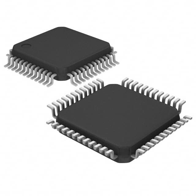
The IC is housed in a 48-LQFP package with an alternative supplier device package of 48-TQFP (7x7 mm). It is surface mount and operates over a temperature range of -40°C to 85°C. The device is RoHS3 compliant and has a moisture sensitivity level of MSL 3 (168 hours).
It includes a divider function (multiplier not present). With one PLL circuit and bypass capability, it offers flexibility in clock generation. The product is currently marked as obsolete by the manufacturer.
3.135V to 3.465V.
48-LQFP, also listed as supplier device package 48-TQFP (7x7 mm).
-40°C to 85°C.
Yes, RoHS3 compliant.
Yes, with bypass capability.
625 MHz.
LVDS and LVPECL differential outputs.