

| Distributor | Stock | Pricing | MOQ | PKG | Lead Time | Date Code | On Order Quantity | On Order Delivery | |
|---|---|---|---|---|---|---|---|---|---|
|
1,969 pcs
|
1969 pcs | On Request | 1 | On Request | On Request | On Request | On Request | On Request |
| Category | |
| Manufacturer Name | |
| Differential | |
| Frequency | |
| Input | |
| Mounting Type | |
| Number of Circuits | |
| Operating Temperature | |
| Output | |
| Ratio | |
| SVHC Present | |
| Supplier Device Package | |
| Type | |
| Voltage |
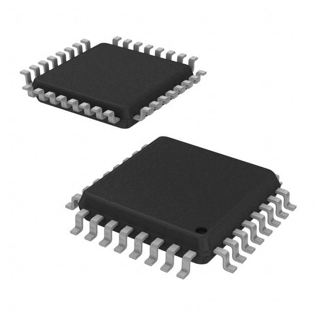
The 83948AYI-147LF is a high-performance clock fanout buffer and multiplexer designed by Renesas. It provides a 2:12 fanout ratio, allowing distribution of clock signals to multiple destinations. The device supports a wide range of input logic standards including HCSL, LVCMOS, LVDS, LVHSTL, LVPECL, LVTTL, and SSTL, while outputs are LVCMOS and LVTTL compatible. With a maximum frequency of 350 MHz, it is suitable for various clock distribution applications.
The device operates from a supply voltage range of 2.375V to 3.465V, making it flexible for different system power rails. It is designed for surface mount assembly and is housed in a 32-LQFP package, with the supplier device package specified as 32-TQFP (7x7). The operating temperature range is -40°C to 85°C, allowing use in industrial environments.
This component is ideal for applications requiring precise clock distribution with low skew and multiple output options. The 2:12 configuration enables efficient fan-out from two input sources to twelve outputs, with multiplexing capability for selecting between inputs.
2.375V to 3.465V.
32-LQFP (supplier device package 32-TQFP 7x7).
-40°C to 85°C.
RoHS3 compliant (unverified).
350 MHz.
HCSL, LVCMOS, LVDS, LVHSTL, LVPECL, LVTTL, SSTL.
2:12.