


| Distributor | Stock | Pricing | MOQ | PKG | Lead Time | Date Code | On Order Quantity | On Order Delivery | |
|---|---|---|---|---|---|---|---|---|---|
|
26,530 pcs
|
26530 pcs | On Request | 1 | On Request | On Request | On Request | On Request | On Request |
| Category | |
| Manufacturer Name | |
| Differential | |
| Frequency | |
| Input | |
| Mounting Type | |
| Number of Circuits | |
| Operating Temperature | |
| Output | |
| Ratio | |
| Supplier Device Package | |
| Type | |
| Voltage |
The Renesas 8316AKLF is a fanout buffer (distribution) integrated circuit designed to distribute one clock input to sixteen separate outputs. With a maximum operating frequency of 150 MHz, it supports LVCMOS and LVTTL logic levels for both input and output signals. The input-to-output ratio is 1:16, and the device provides a single buffer circuit.
Electrical specifications include a supply voltage range of 3.135 V to 3.465 V and an operating temperature range of 0°C to 70°C. The buffer is intended for clock distribution applications where a single LVCMOS/LVTTL clock source must be fanned out to multiple loads while maintaining signal levels.
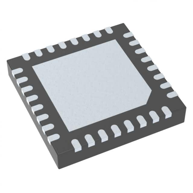
The device is packaged in a 32-VFQFN exposed pad package, with a supplier device package of 32-VFQFPN measuring 5 x 5 mm. It uses surface-mount mounting and is suitable for board-level clock distribution in systems requiring multiple copies of a clock signal.
The supply voltage range is 3.135 V to 3.465 V.
It is offered in a 32-VFQFN Exposed Pad package, with supplier package designation 32-VFQFPN (5x5).
0°C to 70°C.
RoHS3 Compliant (unverified).
150 MHz.
Input and output support LVCMOS and LVTTL logic levels.
1:16.