

| Distributor | Stock | Pricing | MOQ | PKG | Lead Time | Date Code | On Order Quantity | On Order Delivery | |
|---|---|---|---|---|---|---|---|---|---|
|
5,750 pcs
|
5750 pcs | On Request | 1 | On Request | On Request | On Request | On Request | On Request |
| Category | |
| Manufacturer Name | |
| Differential | |
| Divider | |
| Frequency | |
| Input | |
| Mounting Type | |
| Number of Circuits | |
| Operating Temperature | |
| Output | |
| PLL | |
| Ratio | |
| SVHC Present | |
| Supplier Device Package | |
| Type | |
| Voltage |
The Renesas 813N322CKI-02LF is a jitter attenuator integrated circuit designed for clock timing applications. It incorporates a phase-locked loop (PLL) and provides jitter attenuation for high-speed signals. The device accepts differential inputs including HCSL, LVDS, LVHSTL, and LVPECL, and outputs a LVPECL signal. It features a 2:2 input-to-output ratio with differential signaling on both sides. The maximum output frequency is 622.08 MHz. The operating supply voltage range is from 3.135V to 3.465V.
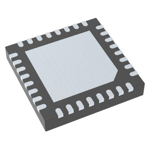
The device includes a divider function but no multiplier. It is housed in a 32-VFQFN exposed pad package with a surface mount mounting type. The supplier device package is 32-VFQFPN (5x5). The operating temperature range is -40°C to 85°C, making it suitable for industrial environments. The IC is RoHS3 compliant (unverified) and has MSL level 1.
This jitter attenuator is ideal for cleaning up clock signals in communication systems, data centers, and networking equipment. Its wide input compatibility allows for easy integration into various designs. The PLL provides jitter reduction, ensuring signal integrity.
3.135V to 3.465V.
-40°C to 85°C.
32-VFQFN Exposed Pad, with supplier package 32-VFQFPN (5x5).
622.08 MHz.
LVPECL.
RoHS3 Compliant (unverified).
HCSL, LVDS, LVHSTL, LVPECL.