

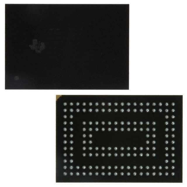
74SSTUB32865AZJBR The Texas Instruments 74SSTUB32865AZJBR is a 28-bit to 56-bit configurable registered buffer designed for 1.7V to 1.9V VCC operation. It features parity testing and operates within an industrial temperature range.
Mfr Part #:

74SSTUB32865AZJBR

Available from 1 distributors
Mfr Name: Texas Instruments
Texas Instruments
The Texas Instruments 74SSTUB32865AZJBR is a 28-bit to 56-bit configurable registered buffer designed for 1.7V to 1.9V VCC operation. It features parity testing and operates within an industrial temperature range.
✓ Total Stock: 2,000 pcs
$ Price Range: $0.50

74SSTUB32865AZJBR Available from 1 distributor

✓ Authorised
✓ Non-Authorised
Distributor Stock Pricing MOQ PKG Lead Time Date Code On Order Quantity On Order Delivery
Non-Authorised Inventory information
2,000 pcs
2000 pcs On Request 1 On Request On Request 1210+ On Request On Request

74SSTUB32865AZJBR Specifications Quick View

Most important parameters for selection – full specs in datasheet.
Category
Manufacturer Name
Logic Type
Mounting Type
Number of Bits
Operating Temperature
SVHC Present
Supplier Device Package
Supply Voltage

74SSTUB32865AZJBR Description

Short technical summary and product information.

The 74SSTUB32865AZJBR from Texas Instruments is a 28-bit to 56-bit configurable registered buffer that supports SSTL_18 data inputs and LVCMOS switching levels. It is designed for 1.7V to 1.9V VCC operation and is a member of the Texas Instruments Widebus+ family.


This device checks parity on DIMM-independent data inputs and indicates parity errors on the PTYERR output. It supports stacked DDR2 RDIMMs, with one device per DIMM driving up to 18 SDRAM loads, or two devices per DIMM driving up to 36 loads. The pinout is optimized for DDR2 RDIMM PCB layout.


The 74SSTUB32865AZJBR operates from a differential clock and registers data at the crossing of CK going high and CK going low. All inputs are SSTL_18, except for the chip-select gate-enable (CSGateEN) and reset (RESET) inputs, which are LVCMOS. All outputs are edge-controlled circuits optimized for unterminated DIMM loads and meet SSTL_18 specifications, except for the open-drain error (PTYERR) output.


Packaged in a 160-TFBGA, this component is suitable for surface mounting and operates across an industrial temperature range of -40°C to 85°C.

74SSTUB32865AZJBR Quick Information

Product Type: Registered Buffer
Series: 74SSTUB
Canonical Name: 28-Bit to 56-Bit Registered Buffer with Address-Parity Test
Subcategory: Registered Buffer

74SSTUB32865AZJBR Compliance

RoHS Status: RoHS Compliant
Moisture Sensitivity Level (MSL): 1 Unlimited
REACH Status: REACH Unaffected

74SSTUB32865AZJBR Estimated Pricing

Qty Low High
1+ $0.50 $0.50

Estimated market price range - modelled values for guidance only, not live distributor offers.

74SSTUB32865AZJBR Features

  • 28-bit to 56-bit configurable registered buffer.
  • Supports SSTL_18 and LVCMOS inputs.
  • Includes address-parity test functionality.
  • Operates at 1.7V to 1.9V supply voltage.
  • Packaged in 160-TFBGA for surface mounting.

74SSTUB32865AZJBR Applications

  • Designed for DDR2 RDIMM applications.
  • Suitable for heavily loaded DIMMs.
  • Used in memory controller interfaces.
  • Supports stacked DDR2 SDRAM loads.

74SSTUB32865AZJBR FAQs

7 frequently asked questions generated from this part’s specifications.
What is the operating voltage range?

1.7V to 1.9V

What is the operating temperature range?

-40°C to 85°C

What is the package type?

160-TFBGA

How many bits does this buffer support?

28 bits

What is the logic type?

1:2 Registered Buffer with Parity

What is the mounting type?

Surface Mount

What is the supplier device package?

160-NFBGA (9x13)

Home
Account

Categories