

| Distributor | Stock | Pricing | MOQ | PKG | Lead Time | Date Code | On Order Quantity | On Order Delivery | |
|---|---|---|---|---|---|---|---|---|---|
|
1,230 pcs
|
1230 pcs | On Request | 1 | On Request | On Request | 0628P// | On Request | On Request |
| Category | |
| Manufacturer Name | |
| Clock Frequency | |
| Input Capacitance | |
| Lead Spacing | |
| Lead Style | |
| Mounting Type | |
| Operating Temperature | |
| Output Current | |
| Propagation Delay | |
| Quiescent Current | |
| SVHC Present | |
| Storage Temperature | |
| Voltage |
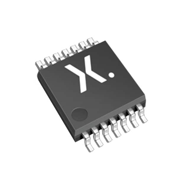
The Nexperia 74LVC74APW is a dual D-type flip-flop designed for data storage and transfer applications. It operates with a supply voltage range of 1.2V to 3.6V and supports a maximum clock frequency of 150MHz.
This component features a 14-TSSOP surface-mount package, making it suitable for various electronic designs. The operating temperature range is from -40°C to 125°C, ensuring reliable performance in diverse environments. Key electrical characteristics include a quiescent current of 10µA and an output current of 24mA.
The 74LVC74APW is part of the 74LVC series, known for its low voltage operation and high performance. Its dual D-type flip-flop configuration allows for independent storage of two bits of data, controlled by a positive edge trigger.
This device is commonly used in digital logic circuits for state holding, data synchronization, and frequency division. Its specifications make it a versatile choice for embedded systems, control units, and data processing applications.
| Qty | Low | High |
|---|---|---|
| 1+ | $0.86 | $0.86 |
Estimated market price range - modelled values for guidance only, not live distributor offers.
The operating temperature range for the 74LVC74APW is -40°C to 125°C.
The supply voltage range for the 74LVC74APW is 1.2V to 3.6V.
The maximum clock frequency of the 74LVC74APW is 150MHz.
The 74LVC74APW is supplied in a 14-TSSOP package.
Common issues can arise from improper power supply voltage, which should be within the recommended range of 1.65V to 5.5V, or incorrect input signal timing between the clock and data inputs.