

| Distributor | Stock | Pricing | MOQ | PKG | Lead Time | Date Code | On Order Quantity | On Order Delivery | |
|---|---|---|---|---|---|---|---|---|---|
|
359 pcs
|
359 pcs | On Request | 1 | On Request | On Request | On Request | On Request | On Request | |
|
359 pcs
|
359 pcs | On Request | 1 | On Request | On Request | On Request | On Request | On Request | |
|
55 pcs
|
55 pcs | On Request | 1 | On Request | On Request | On Request | On Request | On Request |
| Category | |
| Manufacturer Name | |
| Current | |
| Input Logic Level | |
| Lead Style | |
| Logic Type | |
| Max Propagation Delay @ V, Max CL | |
| Mounting Type | |
| Number of Circuits | |
| Number of Inputs | |
| Operating Temperature | |
| Supplier Device Package | |
| Supplier Package | |
| Voltage |
The 74LVC1G08GW,125 is a single 2-input AND gate from NXP Semiconductors. It is designed for applications requiring a wide supply voltage range, from 1.65 V to 5.5 V, allowing for use in mixed 3.3 V and 5 V systems.
This device features Schmitt trigger action on its inputs, providing tolerance for slower input rise and fall times. It offers a propagation delay of 4 ns at 5V with a 50pF load capacitance. The output drive current is ±24 mA at 3.0 V.
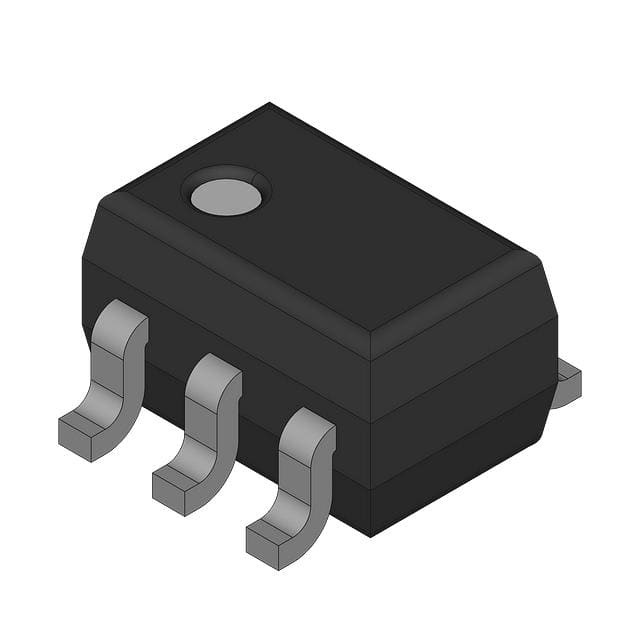
The 74LVC1G08GW,125 is available in a 5-TSSOP package and is designed for surface mount applications. It operates within a temperature range of -40°C to +125°C (TA). The part is specified for partial power-down applications using IOFF circuitry.
Key electrical characteristics include a supply voltage range of 1.65V to 5.5V and an input logic level range of 1.7V to 2V. The device is suitable for TTL level interfacing and offers overvoltage tolerant inputs up to 5.5V.
| Qty | Low | High |
|---|---|---|
| 1+ | $0.22 | $0.22 |
Estimated market price range - modelled values for guidance only, not live distributor offers.
The supply voltage range is 1.65 V to 5.5 V.
The 74LVC1G08GW,125 is available in surface-mount 5-TSSOP, SC-70-5, and SOT-353 packages.
The operating temperature range is -40°C to +125°C.
The maximum propagation delay is 4 ns at 5V and 50pF load.
The output drive current is ±24 mA typical at VCC = 3.0 V.
The 74LVC1G08GW,125 contains one circuit with two inputs.
The input logic levels are specified from 1.7 V to 2 V.