

| Distributor | Stock | Pricing | MOQ | PKG | Lead Time | Date Code | On Order Quantity | On Order Delivery | |
|---|---|---|---|---|---|---|---|---|---|
|
50 pcs
|
50 pcs | On Request | 1 | On Request | On Request | On Request | On Request | On Request |
| Category | |
| Manufacturer Name | |
| AEC Qualified | |
| Automotive Grade | |
| Circuit | |
| Current | |
| Independent Circuits | |
| Industrial Grade | |
| Lead Spacing | |
| Lead Style | |
| Medical Grade | |
| Military Grade | |
| Mounting Type | |
| Operating Temperature | |
| SVHC Present | |
| Supplier Device Package | |
| Tape & Reel | |
| Type | |
| Voltage | |
| Voltage Supply Source |
The 74HC257N,652 from NXP Semiconductors is a high-speed Si-gate CMOS device that functions as a quad 2-input multiplexer with 3-state outputs. It is pin-compatible with Low-power Schottky TTL (LSTTL).
This multiplexer selects 4 bits of data from two sources, controlled by a common data select input (S). Data inputs from source 0 are selected when S is LOW, and data inputs from source 1 are selected when S is HIGH. The outputs (1Y to 4Y) present data in true (non-inverting) form. The outputs are forced to a high-impedance OFF-state when the Output Enable (OE) is HIGH.
Key features include a non-inverting data path and 3-state outputs that interface directly with a system bus. The device complies with JEDEC standard no. 7A and offers robust ESD protection, exceeding 2000V for HBM and 200V for MM.
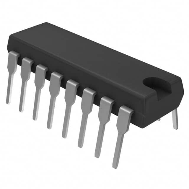
Available in a 16-DIP package, the 74HC257N,652 is specified for operation from -40°C to +125°C. It operates from a single supply voltage ranging from 2V to 6V, with a typical quiescent current of 7.8mA.
| Qty | Low | High |
|---|---|---|
| 1+ | $0.50 | $0.50 |
Estimated market price range - modelled values for guidance only, not live distributor offers.
2V to 6V single supply.
16-DIP (0.300", 7.62mm) through-hole package.
-40°C to 125°C.
4 x 2:1 multiplexer.
Through hole mounting.
HBM exceeds 2000V, MM exceeds 200V.