

| Distributor | Stock | Pricing | MOQ | PKG | Lead Time | Date Code | On Order Quantity | On Order Delivery | |
|---|---|---|---|---|---|---|---|---|---|
|
3,200 pcs
|
3200 pcs | On Request | 1 | On Request | On Request | On Request | On Request | On Request |
| Category | |
| Manufacturer Name | |
| Differential | |
| Frequency | |
| Input | |
| Mounting Type | |
| Number of Circuits | |
| Operating Temperature | |
| Output | |
| Ratio | |
| SVHC Present | |
| Supplier Device Package | |
| Type | |
| Voltage |
The 74FCT38072DCGI is a clock fanout buffer IC from Renesas designed for distributing a single clock input to two outputs. It features a 1:2 ratio, accepts LVTTL input levels, and provides LVCMOS and LVTTL compatible outputs. The device operates at a maximum frequency of 166 MHz, making it suitable for a variety of clock distribution applications in digital systems.
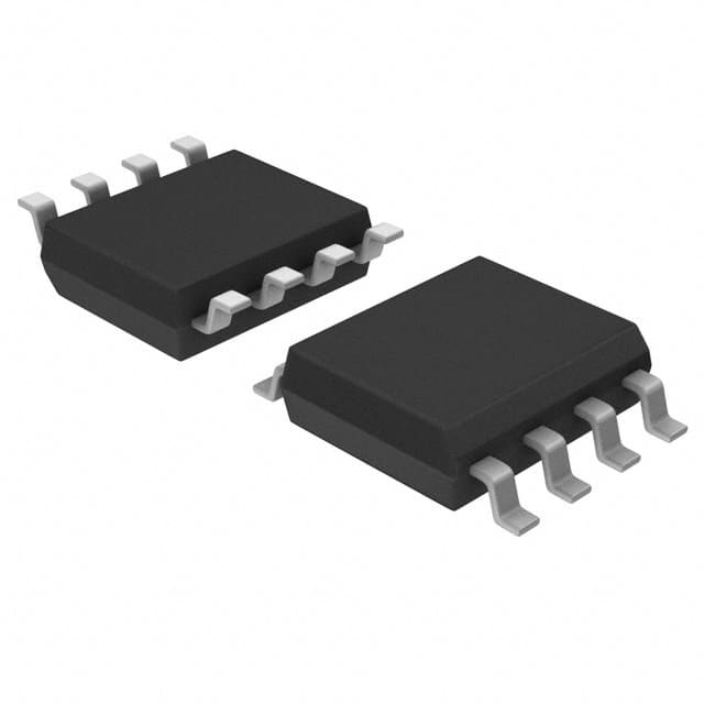
The buffer operates from a supply voltage range of 3V to 3.6V and is specified over an industrial temperature range of -40°C to 85°C. The input and output are non-differential, simplifying system design in single-ended clock environments. The part is mounted in a standard 8-SOIC surface-mount package with a 0.154-inch body width and 3.90mm lead pitch.
The 74FCT38072DCGI is part of the 74FCT series and is offered in tube packaging. Its compact footprint and low-voltage operation make it a practical choice for board-level clock buffering and fanout expansion in communication, computing, and industrial equipment.
The supply voltage range is 3V to 3.6V.
It is available in an 8-SOIC (0.154", 3.90mm width) surface-mount package.
The operating temperature range is -40°C to 85°C.
RoHS status is listed as RoHS3 compliant, but this is unverified.
The maximum frequency is 166 MHz.
The ratio is 1:2, meaning one input drives two outputs.
Input is LVTTL; outputs are LVCMOS or LVTTL.