

| Distributor | Stock | Pricing | MOQ | PKG | Lead Time | Date Code | On Order Quantity | On Order Delivery | |
|---|---|---|---|---|---|---|---|---|---|
|
2,396 pcs
|
2396 pcs | On Request | 1 | On Request | On Request | On Request | On Request | On Request | |
|
1,094 pcs
|
1094 pcs | On Request | 1 | On Request | On Request | 01+ | On Request | On Request |
| Category | |
| Manufacturer Name | |
| AEC Qualified | |
| Automotive Grade | |
| Current | |
| Industrial Grade | |
| Input Logic Level | |
| Logic Type | |
| Max Propagation Delay @ V, Max CL | |
| Medical Grade | |
| Military Grade | |
| Mounting Type | |
| Number of Circuits | |
| Number of Inputs | |
| Operating Temperature | |
| Supplier Device Package | |
| Tape & Reel | |
| Voltage |
The 74F04SCX is a Hex Inverter integrated circuit manufactured by ON Semiconductor. This device contains six independent inverter gates, each performing the logic NOT function. It is designed to operate with a supply voltage ranging from 4.5V to 5.5V.
The 74F04SCX features a maximum propagation delay of 5ns at 5V and 50pF load capacitance. The output current capabilities are 1mA for high output and 20mA for low output. Input logic levels are recognized as HIGH at 2V and LOW at 0.8V.
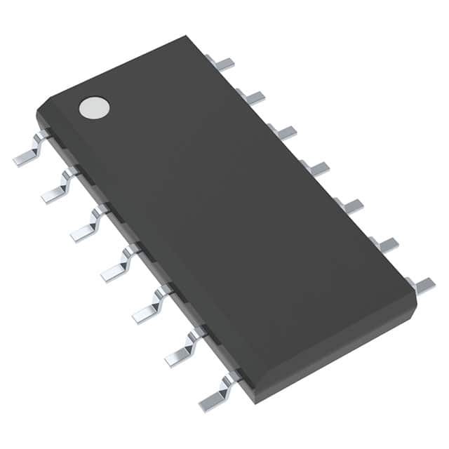
This component is housed in a 14-SOIC (Small Outline Integrated Circuit) package, suitable for surface mounting. The operating temperature range is from 0°C to 70°C, making it suitable for various commercial applications. The device is RoHS3 compliant.
With its six independent inverters, the 74F04SCX is a versatile component for digital logic designs requiring signal inversion. Its standard logic family characteristics and SOIC packaging make it compatible with many automated assembly processes.
| Qty | Low | High |
|---|---|---|
| 1+ | $0.22 | $0.22 |
Estimated market price range - modelled values for guidance only, not live distributor offers.
The supply voltage range is 4.5V to 5.5V.
The 74F04SCX is available in a 14-SOIC (0.154", 3.90mm Width) surface-mount package.
The operating temperature range is 0°C to 70°C.
The input high voltage (VIH) minimum is 2.0V, and input low voltage (VIL) maximum is 0.8V.
The maximum propagation delay is 7.0ns for tPLH and 6.5ns for tPHL at 5V and 50pF load.
The output can source 1mA (IOH) and sink 20mA (IOL).
The device contains 6 inverter circuits, each with 1 input.