

| Distributor | Stock | Pricing | MOQ | PKG | Lead Time | Date Code | On Order Quantity | On Order Delivery | |
|---|---|---|---|---|---|---|---|---|---|
|
4,020 pcs
|
4020 pcs | On Request | 1 | On Request | On Request | On Request | On Request | On Request |
| Category | |
| Manufacturer Name | |
| Current | |
| Halogen Free | |
| Input Type | |
| Logic Type | |
| Mounting Type | |
| Number of Bits per Element | |
| Number of Elements | |
| Operating Temperature | |
| Output Type | |
| Supplier Device Package | |
| Voltage |
The 74AUP2G17DW-7 from Diodes Incorporated is part of the Advanced Ultra Low Power (AUP) CMOS logic family, engineered for extended battery life in portable devices. This dual Schmitt trigger buffer operates from a supply voltage range of 0.8V to 3.6V, making it suitable for a variety of low-voltage applications.
Key electrical characteristics include a low static power consumption of less than 0.9µA and a typical dynamic power consumption of 4pF at 3.6V. The device provides ±4mA output drive at 3.0V. The Schmitt trigger action at all inputs enhances tolerance for slower input rise and fall times, improving circuit reliability.
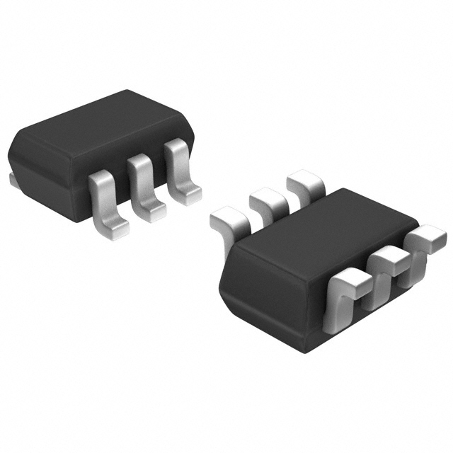
Designed for leadless package applications, the 74AUP2G17DW-7 is available in the SOT-363 package, a surface-mount type. It supports partial power-down operation with I OFF circuitry to prevent damaging current backflow when the device is powered down. ESD protection exceeds 2000V Human Body Model.
This buffer is well-suited for battery-powered products and a wide array of consumer electronics, including PCs, networking equipment, mobile devices, and entertainment systems.
| Qty | Low | High |
|---|---|---|
| 1+ | $0.08 | $0.08 |
Estimated market price range - modelled values for guidance only, not live distributor offers.
The 74AUP2G17DW-7 operates over a supply voltage range of 0.8V to 3.6V.
It is available in a 6-TSSOP, SC-88, or SOT-363 package, with the supplier device package being SOT-363.
The operating temperature range (TA) is -40°C to 125°C.
It has Schmitt trigger inputs, providing noise immunity and hysteresis.
The typical output drive current is ±4mA at 3.0V supply.
The maximum quiescent current (ICC) is less than 0.9µA.
It exceeds 2000V Human Body Model, 200V Machine Model, and 1000V Charged Device Model per JESD 22 standards.