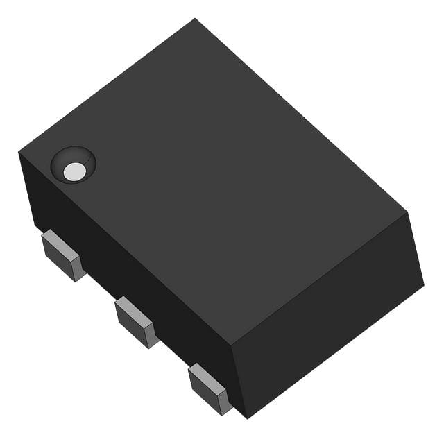
74AUP1G08GS,132 The Nexperia 74AUP1G08GS,132 is a single 2-input AND gate designed for low power dissipation. It operates across a wide supply voltage range from 0.8 V to 3.6 V.
Mfr Part #:

74AUP1G08GS,132

Available from 1 distributors
Mfr Name: NXP Semiconductors
NXP Semiconductors
The Nexperia 74AUP1G08GS,132 is a single 2-input AND gate designed for low power dissipation. It operates across a wide supply voltage range from 0.8 V to 3.6 V.
✓ Total Stock: 45 pcs
$ Price Range: $0.22

74AUP1G08GS,132 Available from 1 distributor

✓ Authorised
✓ Non-Authorised
Distributor Stock Pricing MOQ PKG Lead Time Date Code On Order Quantity On Order Delivery
Non-Authorised Inventory information
45 pcs
45 pcs On Request 1 On Request On Request On Request On Request On Request

74AUP1G08GS,132 Specifications Quick View

Most important parameters for selection – full specs in datasheet.
Category
Manufacturer Name
Latch-up Performance
Lead Style
Mounting Type

74AUP1G08GS,132 Description

Short technical summary and product information.

The 74AUP1G08 is a single 2-input AND gate from Nexperia, offering very low static and dynamic power consumption across its wide supply voltage range of 0.8 V to 3.6 V. Its Schmitt-trigger action at all inputs provides tolerance for slower input rise and fall times, enhancing noise immunity.


This device is fully specified for partial power-down applications using its IOFF circuitry, which prevents damaging backflow current when the device is powered down. It boasts low static power consumption with a maximum ICC of 0.9 μA. The inputs are overvoltage tolerant up to 3.6 V, and it exhibits low noise overshoot and undershoot, typically less than 10% of VCC.


Available in multiple package options including TSSOP5 and various XSON6 and X2SON5 variants, the 74AUP1G08 is suitable for space-constrained applications. It meets various JEDEC standards for different voltage ranges and offers robust ESD protection exceeding 5000 V for HBM and 1000 V for CDM.


Key features include wide supply voltage operation, CMOS low power dissipation, high noise immunity, and IOFF circuitry for power-down mode. Latch-up performance exceeds 100 mA per JESD 78 Class II Level B. The device is specified for operation in temperature ranges of -40 °C to +85 °C and -40 °C to +125 °C.

74AUP1G08GS,132 Quick Information

Product Type: AND Gate
Series: 74AUP1G08
Canonical Name: 74AUP1G08 Single 2-Input AND Gate
Subcategory: AND Gate

74AUP1G08GS,132 Compliance

RoHS Status: RoHS Compliant
Moisture Sensitivity Level (MSL): 1 Unlimited
REACH Status: REACH Unaffected

74AUP1G08GS,132 Estimated Pricing

Qty Low High
1+ $0.22 $0.22

Estimated market price range - modelled values for guidance only, not live distributor offers.

74AUP1G08GS,132 Features

  • Wide 0.8 V to 3.6 V supply voltage range.
  • Very low static and dynamic power consumption.
  • Schmitt-trigger action at all inputs.
  • IOFF circuitry for partial power-down.
  • High noise immunity and overvoltage tolerance.

74AUP1G08GS,132 Applications

  • Low-power digital logic circuits.
  • Battery-powered electronic devices.
  • Portable consumer electronics.
  • Signal gating and control applications.

74AUP1G08GS,132 FAQs

6 frequently asked questions generated from this part’s specifications.
What is the operating voltage range for the 74AUP1G08GS,132?

The 74AUP1G08GS,132 operates across a wide supply voltage range from 0.8 V to 3.6 V.

What is the static power consumption of this AND gate?

The maximum static power consumption (ICC) for the 74AUP1G08GS,132 is 0.9 μA.

Does the 74AUP1G08GS,132 have Schmitt-trigger inputs?

Yes, the 74AUP1G08GS,132 features Schmitt-trigger action at all inputs.

What temperature range is the 74AUP1G08GS,132 specified for?

The device is specified for operation from -40 °C to +125 °C.

What ESD protection is provided for the 74AUP1G08GS,132?

It offers Human Body Model (HBM) ESD protection exceeding 5000 V and Charged Device Model (CDM) protection exceeding 1000 V.

What is the latch-up performance of the 74AUP1G08GS,132?

The latch-up performance exceeds 100 mA per JESD 78 Class II Level B.

74AUP1G08GS,132 Alternate Parts

Same form/fit/function or matching attribute configuration across different manufacturers.
View All Alternate Parts
SN74AUC1G08DBVR
SN74AUC1G08DBVR
Texas Instruments
The Texas Instruments SN74AUC1G08DBVR is a single 2-input positive-AND gate. It operates from 0.8V to 2.7V and features a maximum propagation delay of 2.4 ns at 1.8V.

View Part
74AUP1G11GW,125
74AUP1G11GW,125
Nexperia USA Inc.
The Nexperia 74AUP1G11GW,125 is a single 3-input AND gate. It operates over a wide supply voltage range and offers low static power consumption.
View Part
74HCT1G08GV,125
74HCT1G08GV,125
Nexperia USA Inc.
The 74HCT1G08GV,125 is a single 2-input AND gate from Nexperia, operating from 2V to 6V with a typical propagation delay of 27ns at 4.5V.
View Part
74HCT00D,652
74HCT00D,652
NXP Semiconductors
The NXP Semiconductors 74HCT00D,652 is a Quad 2-input NAND Gate. It operates over a wide supply voltage range and is specified for extended temperature ranges.
View Part
Home
Account

Categories