

| Distributor | Stock | Pricing | MOQ | PKG | Lead Time | Date Code | On Order Quantity | On Order Delivery | |
|---|---|---|---|---|---|---|---|---|---|
|
3,600 pcs
|
3600 pcs | On Request | 1 | On Request | On Request | On Request | On Request | On Request |
| Category | |
| Manufacturer Name | |
| Differential | |
| Frequency | |
| Input | |
| Main Purpose | |
| Mounting Type | |
| Number of Circuits | |
| Operating Temperature | |
| Output | |
| PLL | |
| Ratio | |
| Supplier Device Package | |
| Voltage |
The Renesas 6V31021NLGI is a 1:4 fanout clock buffer IC designed for application-specific timing requirements in Ethernet and PCI Express systems. It accepts a single LVCMOS input and provides four LVCMOS outputs with differential capability, supporting both input and output differential signals. The device operates over a frequency range up to 167 MHz, with a supply voltage range of 3V to 3.6V.
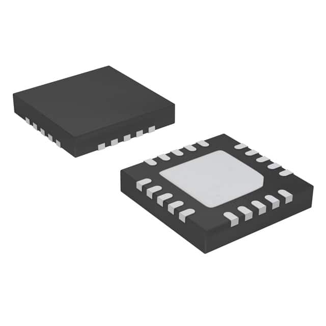
This clock buffer is housed in a 20-VFQFN exposed pad package (20-QFN 4x4 mm) and is surface mountable. It is specified for an operating temperature range of -40°C to +85°C, making it suitable for industrial environments. The 1:4 ratio allows distribution of a single clock signal to multiple destinations while maintaining signal integrity.
The part is intended for use in Ethernet switches, routers, and PCIe clock distribution applications where low-skew, low-jitter clock buffering is required. The LVCMOS interface ensures compatibility with common digital logic families. The device does not include an internal PLL, so it provides a simple buffering function without frequency synthesis.
3V to 3.6V.
20-VFQFN Exposed Pad (20-QFN 4x4 mm).
-40°C to +85°C.
RoHS3 Compliant.
167 MHz.
LVCMOS for both input and output.
Yes, both input and output support differential signals.