

| Distributor | Stock | Pricing | MOQ | PKG | Lead Time | Date Code | On Order Quantity | On Order Delivery | |
|---|---|---|---|---|---|---|---|---|---|
|
9,209 pcs
|
9209 pcs | On Request | 1 | On Request | On Request | On Request | On Request | On Request | |
|
3,222 pcs
|
3222 pcs | On Request | 1 | On Request | On Request | On Request | On Request | On Request | |
| On Request | On Request | 1 | On Request | On Request | On Request | On Request | On Request |
| Category | |
| Manufacturer Name | |
| Differential | |
| Divider | |
| Frequency | |
| Input | |
| Mounting Type | |
| Number of Circuits | |
| Operating Temperature | |
| Output | |
| PLL | |
| Ratio | |
| SVHC Present | |
| Supplier Device Package | |
| Voltage |
The Renesas 5V9885TPFGI is a versatile clock generator IC designed for high-performance timing applications. It integrates a phase-locked loop (PLL) with bypass capability, allowing flexible clock synthesis or direct feed-through. The device accepts LVCMOS or LVTTL inputs and provides six outputs configurable as LVCMOS, LVDS, LVPECL, or LVTTL levels, supporting differential signaling on the output side.
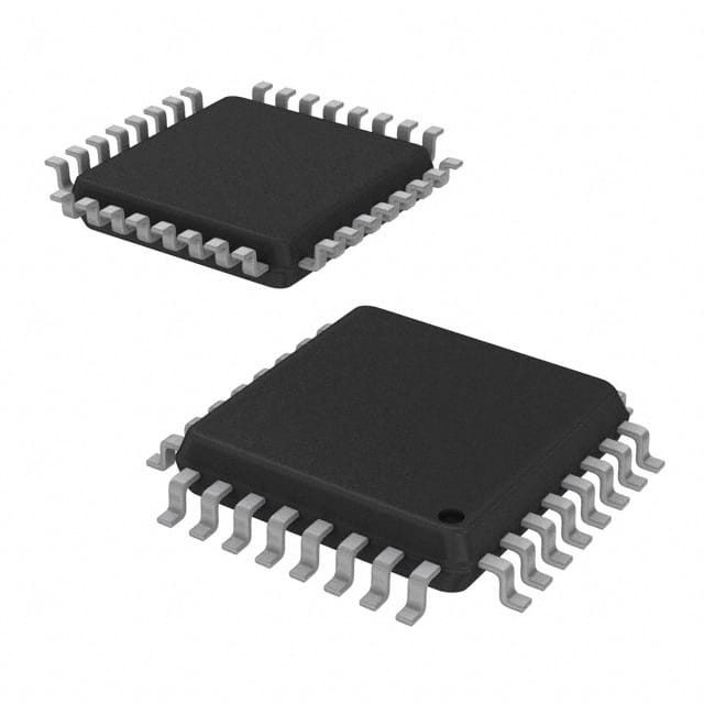
Operating from a 3V to 3.6V supply, the 5V9885TPFGI can generate clocks up to 500MHz. It includes both divider and multiplier functions with a 2:6 input-to-output ratio, making it suitable for frequency scaling and jitter cleaning. The device is rated for industrial temperature range (-40°C to +85°C) and comes in a compact 32-lead LQFP package (32-TQFP 7x7mm), suitable for surface mount assembly.
This clock generator is ideal for networking, telecom, FPGA, and ASIC timing solutions where low-jitter, multiple output formats, and programmable frequency synthesis are required. The package is RoHS3 compliant and has an MSL rating of 3 (168 hours floor life).
The supply voltage range is 3V to 3.6V.
It comes in a 32-lead LQFP package (32-TQFP, 7x7mm).
The operating temperature range is -40°C to +85°C.
Yes, it is RoHS3 compliant.
It supports LVCMOS, LVDS, LVPECL, and LVTTL outputs.
Yes, it has an integrated PLL with bypass capability.
The maximum output frequency is 500 MHz.