

| Distributor | Stock | Pricing | MOQ | PKG | Lead Time | Date Code | On Order Quantity | On Order Delivery | |
|---|---|---|---|---|---|---|---|---|---|
|
19 pcs
|
19 pcs | On Request | 1 | On Request | On Request | On Request | On Request | On Request |
| Category | |
| Manufacturer Name | |
| Data Rate | |
| Failure Rate | |
| Mounting Type | |
| Number of I | |
| Number of LABs | |
| Number of Logic Elements | |
| Operating Temperature | |
| SVHC Present | |
| Supplier Device Package | |
| Total RAM Bits | |
| Voltage |
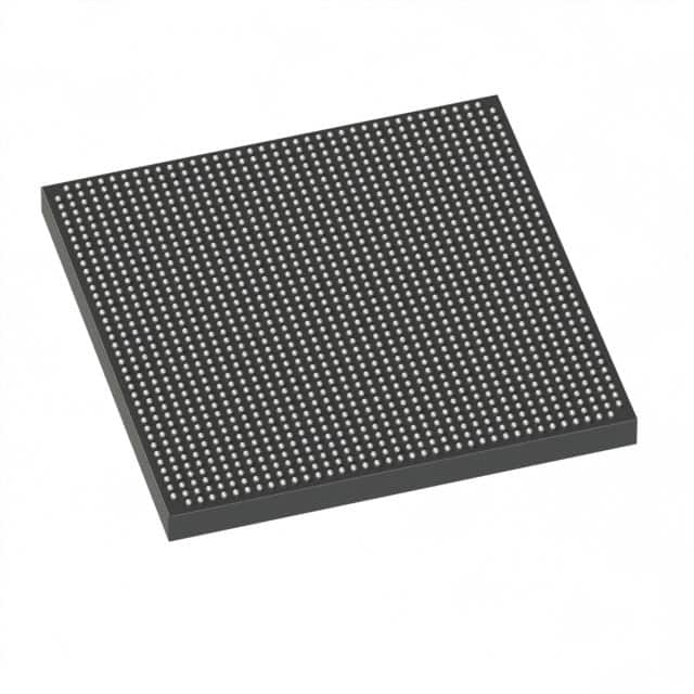
The Intel 5SGXMABK2H40C3N is a Stratix V GX Field Programmable Gate Array (FPGA) from Intel's Stratix V family. It features 952,000 logic elements, 359,200 logic array blocks (LABs), and 53,248,000 bits of embedded memory. With 696 general-purpose I/O pins and 36 high-speed transceivers capable of up to 14.1 Gbps, this FPGA is suited for high-bandwidth applications. The device operates at a nominal supply voltage of 0.88 V (0.82 V to 0.88 V) and is specified for 0°C to 85°C junction temperature. It comes in a 1517-ball HBGA package (45x45 mm) and is surface mount. Compliance includes RoHS and REACH (unaffected), with MSL level 1 (unlimited). This part is from the Stratix V GX series with speed grade 3. It is supplied in tray packaging. The FPGA's high logic density and transceiver count make it ideal for communications, data center, and high-performance computing applications.
952,000 logic elements.
0.82 V to 0.88 V, nominal 0.88 V.
1517-BBGA, FCBGA (supplier device package 1517-HBGA 45x45).
Speed grade 3.
696 I/O pins.
14.1 Gbps.
53,248,000 bits (62.96 Mb).