

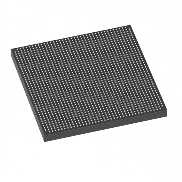
5SGXEA7K2F40I3N Intel Stratix V GX FPGA with 622,000 logic elements, 696 I/O pins, and 51.2 Mb embedded memory. Surface mount in a 1517-ball FBGA package for high-performance applications.
Mfr Part #:

5SGXEA7K2F40I3N

Available from 1 distributors
Mfr Name: Intel
Intel
Intel Stratix V GX FPGA with 622,000 logic elements, 696 I/O pins, and 51.2 Mb embedded memory. Surface mount in a 1517-ball FBGA package for high-performance applications.
✓ Total Stock: 2 pcs

5SGXEA7K2F40I3N Available from 1 distributor

✓ Authorised
✓ Non-Authorised
Distributor Stock Pricing MOQ PKG Lead Time Date Code On Order Quantity On Order Delivery
Non-Authorised Inventory information
2 pcs
2 pcs On Request 1 On Request On Request On Request On Request On Request

5SGXEA7K2F40I3N Specifications Quick View

Most important parameters for selection – full specs in datasheet.
Category
Manufacturer Name
Failure Rate
Mounting Type
Number of I
Number of LABs
Number of Logic Elements
Operating Temperature
Supplier Device Package
Total RAM Bits
Voltage

5SGXEA7K2F40I3N Description

Short technical summary and product information.

The 5SGXEA7K2F40I3N is an Intel Stratix V GX field-programmable gate array (FPGA) designed for high-performance embedded and signal processing systems. It features 622,000 logic elements arranged in 234,720 logic array blocks (LABs) and 51.2 Mb of embedded RAM for data buffering and storage.


The device offers 696 user I/O pins for flexible connectivity and operates from a supply voltage of 0.82V to 0.88V, enabling efficient power consumption. It is rated for industrial temperature range from -40°C to 100°C junction temperature, making it suitable for harsh environments.


The FPGA is packaged in a 1517-ball surface-mount FBGA (40x40 mm) and supports high-speed transceivers as part of the Stratix V GX family. Applications include telecommunications, data centers, high-speed networking, radar, medical imaging, scientific instrumentation, and military/aerospace systems where reconfigurable logic and high throughput are required.

5SGXEA7K2F40I3N Quick Information

Product Type: FPGA (Field Programmable Gate Array)
Series: Stratix V GX
Canonical Name: Intel Stratix V GX FPGA 5SGXEA7K2F40I3N
Subcategory: Field Programmable Gate Array

5SGXEA7K2F40I3N Compliance

RoHS Status: RoHS Compliant
Moisture Sensitivity Level (MSL): 1 Unlimited
REACH Status: REACH Unaffected

5SGXEA7K2F40I3N Features

  • 622,000 logic elements for complex designs.
  • 696 user I/O pins for versatile connectivity.
  • 51.2 Mb embedded memory for data buffering.
  • 0.82V to 0.88V low voltage operation.
  • Industrial temperature range from -40°C to 100°C.

5SGXEA7K2F40I3N Applications

  • Ideal for high-performance telecommunications systems.
  • Used in data center networking equipment.
  • Suitable for radar and medical imaging.
  • Deployed in scientific instrumentation applications.

5SGXEA7K2F40I3N FAQs

7 frequently asked questions generated from this part’s specifications.
How many logic elements does the 5SGXEA7K2F40I3N have?

622,000 logic elements.

What is the number of I/O pins?

696 user I/O pins.

What is the supply voltage range?

0.82V to 0.88V.

What package is used for the 5SGXEA7K2F40I3N?

1517-BBGA, FCBGA (1517-FBGA 40x40 mm).

How much embedded RAM does this FPGA have?

51.2 Mb (51,200,000 bits) of total RAM.

What is the operating temperature range?

-40°C to 100°C junction temperature.

Is the 5SGXEA7K2F40I3N a surface mount device?

Yes, it is surface mount in a 1517-FBGA package.

Home

Categories