

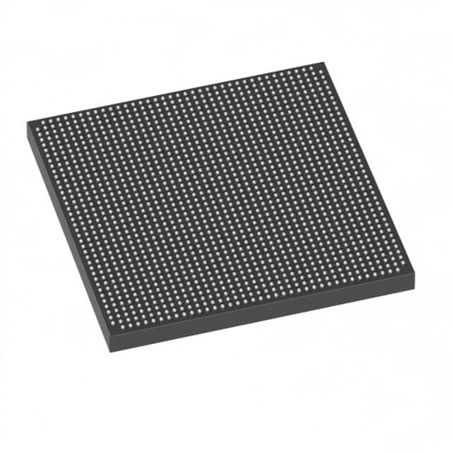
5SGSMD8K3F40C2N Intel Stratix V GS FPGA with 695,000 logic elements, 696 I/O pins, and 51.2 Mb embedded RAM. Surface mount in 1517-FBGA package.
Mfr Part #:

5SGSMD8K3F40C2N

Available from 2 distributors
Mfr Name: Intel
Intel
Intel Stratix V GS FPGA with 695,000 logic elements, 696 I/O pins, and 51.2 Mb embedded RAM. Surface mount in 1517-FBGA package.
✓ Total Stock: 227 pcs

5SGSMD8K3F40C2N Available from 2 distributors

✓ Authorised
✓ Non-Authorised
Distributor Stock Pricing MOQ PKG Lead Time Date Code On Order Quantity On Order Delivery
Non-Authorised Inventory information
117 pcs
117 pcs On Request 1 On Request On Request On Request On Request On Request
Non-Authorised Inventory information
110 pcs
110 pcs On Request 1 On Request On Request 18+ On Request On Request

5SGSMD8K3F40C2N Specifications Quick View

Most important parameters for selection – full specs in datasheet.
Category
Manufacturer Name
Failure Rate
Mounting Type
Number of I
Number of LABs
Number of Logic Elements
Operating Temperature
Supplier Device Package
Total RAM Bits
Voltage

5SGSMD8K3F40C2N Description

Short technical summary and product information.

The Intel 5SGSMD8K3F40C2N is a Stratix V GS series FPGA offering 695,000 logic elements and 262,400 logic array blocks. It features 696 general-purpose I/O pins and 51.2 Mb of total RAM bits. The device operates from a 0.87V to 0.93V supply and is rated for 0°C to 85°C junction temperature. It is housed in a 1517-ball FBGA package (40x40 mm) and is surface mount compatible. This FPGA is designed for high-performance applications such as networking, data centers, and video processing. Note that this part is obsolete and not RoHS compliant.

5SGSMD8K3F40C2N Quick Information

Product Type: FPGA (Field Programmable Gate Array)
Series: Stratix V GS
Canonical Name: Intel Stratix V GS FPGA 5SGSMD8K3F40C2N
Subcategory: Field Programmable Gate Array

5SGSMD8K3F40C2N Compliance

RoHS Status: RoHS Compliant
Moisture Sensitivity Level (MSL): 4 (72 Hours)
REACH Status: REACH Unaffected

5SGSMD8K3F40C2N Features

  • 695,000 logic elements for complex designs.
  • 696 I/O pins for high connectivity.
  • 51.2 Mb embedded RAM for data buffering.
  • 0.87V-0.93V core voltage for low power.
  • 1517-FBGA package for high pin count.

5SGSMD8K3F40C2N Applications

  • Used in high-speed networking equipment.
  • Suitable for data center acceleration.
  • Ideal for video and image processing.
  • Deployed in telecommunications infrastructure.

5SGSMD8K3F40C2N FAQs

7 frequently asked questions generated from this part’s specifications.
How many logic elements does the 5SGSMD8K3F40C2N have?

695,000 logic elements.

How many I/O pins are available?

696 I/O pins.

What is the operating voltage range?

0.87V to 0.93V.

What package is this FPGA available in?

1517-BBGA, FCBGA; supplier device package 1517-FBGA (40x40).

What is the core speed grade?

Speed grade 2.

How much RAM does it have?

51,200,000 bits (51.2 Mb).

What is the operating temperature range?

0°C to 85°C (junction temperature).

Home
Account

Categories