

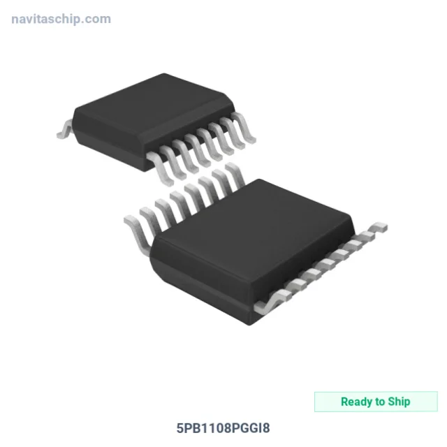
5PB1108PGGI8 The 5PB1108PGGI8 is a 1:8 fanout buffer from Renesas operating at up to 200 MHz with LVCMOS inputs and outputs. It supports multiple supply voltage ranges and comes in a 16-TSSOP package.
Mfr Part #:

5PB1108PGGI8

Available from 1 distributors
Mfr Name: Renesas
Renesas
The 5PB1108PGGI8 is a 1:8 fanout buffer from Renesas operating at up to 200 MHz with LVCMOS inputs and outputs. It supports multiple supply voltage ranges and comes in a 16-TSSOP package.
✓ Total Stock: 44 pcs

5PB1108PGGI8 Available from 1 distributor

✓ Authorised
✓ Non-Authorised
Distributor Stock Pricing MOQ PKG Lead Time Date Code On Order Quantity On Order Delivery
Non-Authorised Inventory information
44 pcs
44 pcs On Request 1 On Request On Request On Request On Request On Request

5PB1108PGGI8 Specifications Quick View

Most important parameters for selection – full specs in datasheet.
Category
Manufacturer Name
Differential
Frequency
Input
Mounting Type
Number of Circuits
Operating Temperature
Output
Ratio
Supplier Device Package
Supplier Package
Type
Voltage

5PB1108PGGI8 Description

Short technical summary and product information.

The 5PB1108PGGI8 is a clock buffer and driver IC manufactured by Renesas Electronics Corporation. It is a fanout buffer (distribution) with a 1:8 input-to-output ratio, designed to distribute a single LVCMOS clock signal to eight LVCMOS outputs. The device operates at a maximum frequency of 200 MHz and supports three supply voltage ranges: 1.71V to 1.89V, 2.375V to 2.625V, and 3.135V to 3.465V.


This buffer is non-differential (single-ended) and comes in a compact 16-TSSOP package with a 4.40mm width. It is surface-mountable and rated for an operating temperature range of -40°C to 85°C. The device is suitable for clock distribution in various electronic systems requiring low-skew, high-speed signal fan-out.


The 5PB1108PGGI8 is supplied in tape and reel packaging. It is RoHS compliant and REACH unaffected. The part is active and available from multiple distributors.

5PB1108PGGI8 Quick Information

Product Type: Clock Buffer
Canonical Name: 5PB1108PGGI8 Clock Buffer 1:8 200MHz 16-TSSOP
Subcategory: Clock Buffer

5PB1108PGGI8 Compliance

RoHS Status: RoHS Compliant
Moisture Sensitivity Level (MSL): 1 Unlimited
REACH Status: REACH Unaffected

5PB1108PGGI8 Features

  • 1:8 fanout buffer for clock distribution.
  • Operates at up to 200 MHz maximum frequency.
  • Supports LVCMOS input and output logic.
  • Wide supply voltage range: 1.71V to 3.465V.
  • Surface-mount 16-TSSOP package.

5PB1108PGGI8 Applications

  • Used in clock distribution for digital systems.
  • Suitable for low-skew signal fan-out.
  • Ideal for FPGA and ASIC clock buffering.
  • Applicable in telecom and networking equipment.

5PB1108PGGI8 FAQs

7 frequently asked questions generated from this part’s specifications.
What is the supply voltage range of the 5PB1108PGGI8?

The device supports three supply voltage ranges: 1.71V to 1.89V, 2.375V to 2.625V, and 3.135V to 3.465V.

What package does the 5PB1108PGGI8 come in?

It comes in a 16-TSSOP package (0.173", 4.40mm Width).

What is the operating temperature range?

The operating temperature range is -40°C to 85°C (TA).

Is the 5PB1108PGGI8 RoHS compliant?

Yes, it is RoHS3 Compliant (unverified).

What is the maximum frequency of the 5PB1108PGGI8?

The maximum frequency is 200 MHz.

What is the input to output ratio?

The input to output ratio is 1:8.

What logic levels does the 5PB1108PGGI8 support?

It supports LVCMOS input and output logic.

Home

Categories