

| Distributor | Stock | Pricing | MOQ | PKG | Lead Time | Date Code | On Order Quantity | On Order Delivery | |
|---|---|---|---|---|---|---|---|---|---|
|
2,645 pcs
|
2645 pcs | On Request | 1 | On Request | On Request | On Request | On Request | On Request |
| Category | |
| Manufacturer Name | |
| Differential | |
| Differential Output | |
| Frequency | |
| Input | |
| Lead Style | |
| Mounting Type | |
| Number of Circuits | |
| Operating Temperature | |
| Output | |
| Ratio | |
| Supplier Device Package | |
| Type | |
| Voltage |
The Renesas 5PB1104CMGI is a 1:4 fanout buffer (distribution) integrated circuit intended for low-skew clock distribution in digital systems. It accepts a single LVCMOS input and provides four identical LVCMOS outputs, making it suitable for buffering and fanout applications.
This device supports a maximum frequency of 200 MHz and operates over a wide supply voltage range of 1.71V to 3.465V. It is a non-differential buffer, with both input and output logic being LVCMOS. The buffer is a single-circuit design with a 1:4 input-to-output ratio.
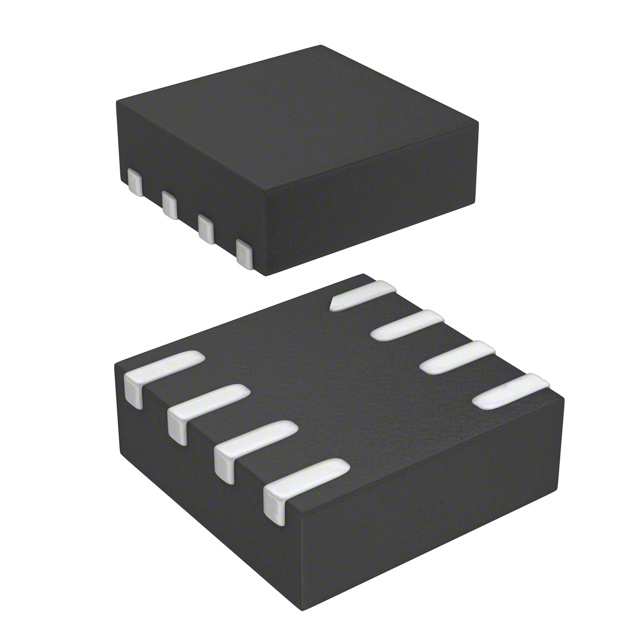
The 5PB1104CMGI is housed in an 8-UFDFN package with a supplier device package of 8-VFQFN (2x2 mm), allowing surface mount assembly. It is rated for an operating temperature range of -40°C to 85°C, making it suitable for industrial environments. The device is RoHS3 compliant and REACH unaffected, though these compliance statuses are based on unverified database records.
The maximum frequency is 200 MHz.
The supply voltage range is 1.71V to 3.465V.
The operating temperature range is -40°C to 85°C.
It comes in an 8-UFDFN package with a supplier device package of 8-VFQFN (2x2 mm).
It is listed as RoHS3 Compliant, though this is unverified.
The input to output ratio is 1:4.
No, both the input and output are non-differential (single-ended LVCMOS).